VISHAY MCL4151 Datasheet

Silicon Epitaxial Planar Diode
Features
D
Electrical data identical with the device 1N4151
D
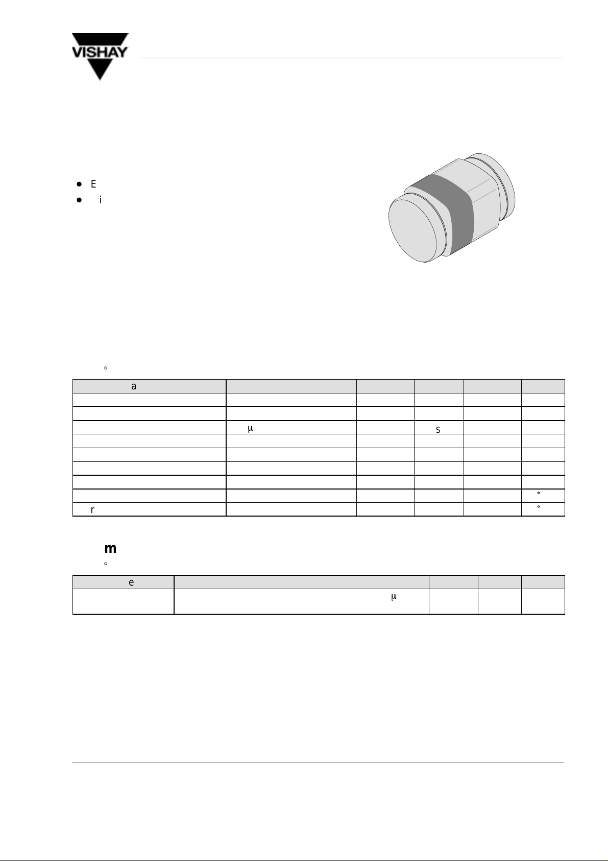
Micro Melf package
Applications
Extreme fast switches
MCL4151
Vishay Telefunken
96 12315
Absolute Maximum Ratings
Tj = 25_C
Parameter Test Conditions Type Symbol Value Unit
Repetitive peak reverse voltage V
Reverse voltage V
Peak forward surge current tp=1ms I
Repetitive peak forward current I
Forward current I
Average forward current VR=0 I
Power dissipation P
Junction temperature T
Storage temperature range T
FSM
FRM
RRM
R
F
FAV
V
j
stg
75 V
50 V
2 A
450 mA
200 mA
150 mA
500 mW
175
–65...+175
Maximum Thermal Resistance
Tj = 25_C
Parameter Test Conditions Symbol Value Unit
Junction ambient mounted on epoxy–glass hard tissue, Fig. 1, 35mm
copper clad, 0.9 mm2 copper area per electrode
R
thJA
500 K/W
°
C
°
C
Document Number 85567
Rev. 3, 01-Apr-99 1 (4)
www.vishay.de • FaxBack +1-408-970-5600

MCL4151
g
y
Vishay Telefunken
Electrical Characteristics
Tj = 25_C
Parameter Test Conditions Type Symbol Min Typ Max Unit
Forward voltage IF=50mA V
Reverse voltage VR=50V I
VR=50V, Tj=150°C I
Breakdown voltage IR=5mA, tp/T=0.01, tp=0.3ms V
Diode capacitance VR=0, f=1MHz, VHF=50mV C
Reverse recovery time IF=IR=10mA, iR=1mA t
IF=10mA, VR=6V, iR=0.1xIR,
R
=100
W
L
Characteristics (Tj = 25_C unless otherwise specified)
0.71 1.3
1.27
Wave Soldering
F
R
R
(BR)
D
rr
t
rr
0.88 1 V
50 nA
50
m
75 V
2 pF
4 ns
2 ns
95 10331
A
25
10
95 10329
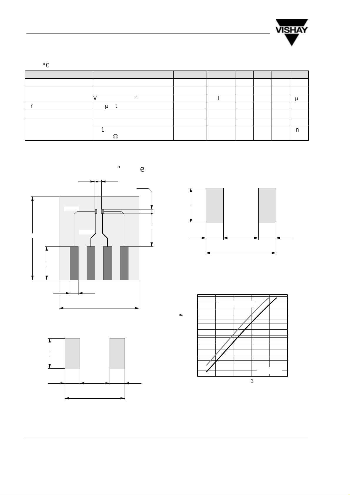
Figure 1. Board for R
Reflow Soldering
1.2
0.152
0.355
2.5
24
definition (in mm)
thJA
0.6 0.6
1.2
2.4
95 10330
9.9
1.4
0.7 0.7
1.4
2.8
Figure 3. Recommended foot pads (in mm)
100
Scattering Limit
10
m
1
0.1
R
I – Reverse Current ( A )
VR=50V
94 9151
0.01
0 40 80 120 160
Tj – Junction Temperature ( °C )
200
Figure 2. Recommended foot pads (in mm)
www.vishay.de • FaxBack +1-408-970-5600 Document Number 85567
Figure 4. Reverse Current vs. Junction Temperature
Rev. 3, 01-Apr-992 (4)
 Loading...