

Vishay MBRS140TRPBF Data Sheet
SMB
Cathode
Vishay High Power Products
Schottky Rectifier, 1.0 A
FEATURES
• Small foot print, surface mountable
• Low forward voltage drop
• High frequency operation
• Guard ring for enhanced ruggedness and long
Anode
term reliability
• Meets MSL level 1, per J-STD-020, LF maximum peak of
260 °C
• Compliant to RoHS directive 2002/95/EC
• Designed and qualified for industrial level
VS-MBRS140TRPbF
PRODUCT SUMMARY
I
F(AV)
V
R
1.0 A
40 V
DESCRIPTION
The VS-MBRS140TRPbF surface mount Schottky rectifier
has been designed for applications requiring low forward
drop and very small foot prints on PC boards. Typical
applications are in disk drives, switching power supplies,
converters, freewheeling diodes, battery charging, and
reverse battery protection.
MAJOR RATINGS AND CHARACTERISTICS
SYMBOL CHARACTERISTICS VALUES UNITS
I
F(AV)
V
I
FSM
V
T
RRM
F
J
Rectangular waveform 1.0 A
40 V
tp = 5 μs sine 380 A
1.0 Apk, TJ = 125 °C 0.53 V
Range - 55 to 150 °C
VOLTAGE RATINGS
PARAMETER SYMBOL VS-MBRS140TRPbF UNITS
Maximum DC reverse voltage V
Maximum working peak reverse voltage V
R
RWM
40 V
ABSOLUTE MAXIMUM RATINGS
PARAMETER SYMBOL TEST CONDITIONS VALUES UNITS
Maximum average forward current I
Maximum peak one cycle
non-repetitive surge current
Non-repetitive avalanche energy E
Repetitive avalanche current I
F(AV)
I
FSM
AR
AS
50 % duty cycle at TL = 119 °C, rectangular waveform 1.0
5 μs sine or 3 μs rect. pulse
10 ms sine or 6 ms rect. pulse 40
TJ = 25 °C, IAS = 1 A, L = 6 mH 3.0 mJ
Current decaying linearly to zero in 1 μs
Frequency limited by T
maximum VA = 1.5 x VR typical
J
Following any rated
load condition and with
rated V
RRM
applied
380
1.0 A
A
Document Number: 94319 For technical questions, contact: diodestech@vishay.com
Revision: 05-Mar-10 1
www.vishay.com
VS-MBRS140TRPbF
Vishay High Power Products
Schottky Rectifier, 1.0 A
ELECTRICAL SPECIFICATIONS
PARAMETER SYMBOL TEST CONDITIONS TYP. MAX. UNITS
1 A
Maximum forward voltage drop V
FM
(1)
1 A
2 A 0.70 0.77
2 A 0.63 0.71
Maximum reverse leakage current I
Maximum junction capacitance C
Typical series inductance L
RM
T
= 125 °C - 4.0
J
VR = 5 VDC (test signal range 100 kHz to 1 MHz), 25 °C - 80 pF
T
S
Measured lead to lead 5 mm from package body - 2.0 nH
TJ = 25 °C
(1)
Maximum voltage rate of change dV/dt Rated V
T
= 25 °C
J
= 125 °C
T
J
V
= Rated V
R
R
R
0.52 0.6
0.48 0.53
-0.1
- 10 000 V/μs
Note
(1)
Pulse width < 300 μs, duty cycle < 2 %
THERMAL - MECHANICAL SPECIFICATIONS
PARAMETER SYMBOL TEST CONDITIONS VALUES UNITS
Maximum junction and storage
temperature range
Maximum thermal resistance,
junction to lead
Maximum thermal resistance,
junction to ambient
Approximate weight
Marking device Case style SMB (similar to DO-214AA) V14
Notes
dP
(1)
------------dT
(2)
Mounted 1" square PCB
1
tot
J
thermal runaway condition for a diode on its own heatsink
--------------<
R
thJA
(1)
T
, T
J
Stg
DC operation
(2)
R
thJL
R
thJA
See fig. 4
DC operation 80
- 55 to 150 °C
36
°C/W
0.10 g
0.003 oz.
V
mA
www.vishay.com For technical questions, contact: diodestech@vishay.com
Document Number: 94319
2 Revision: 05-Mar-10
VS-MBRS140TRPbF
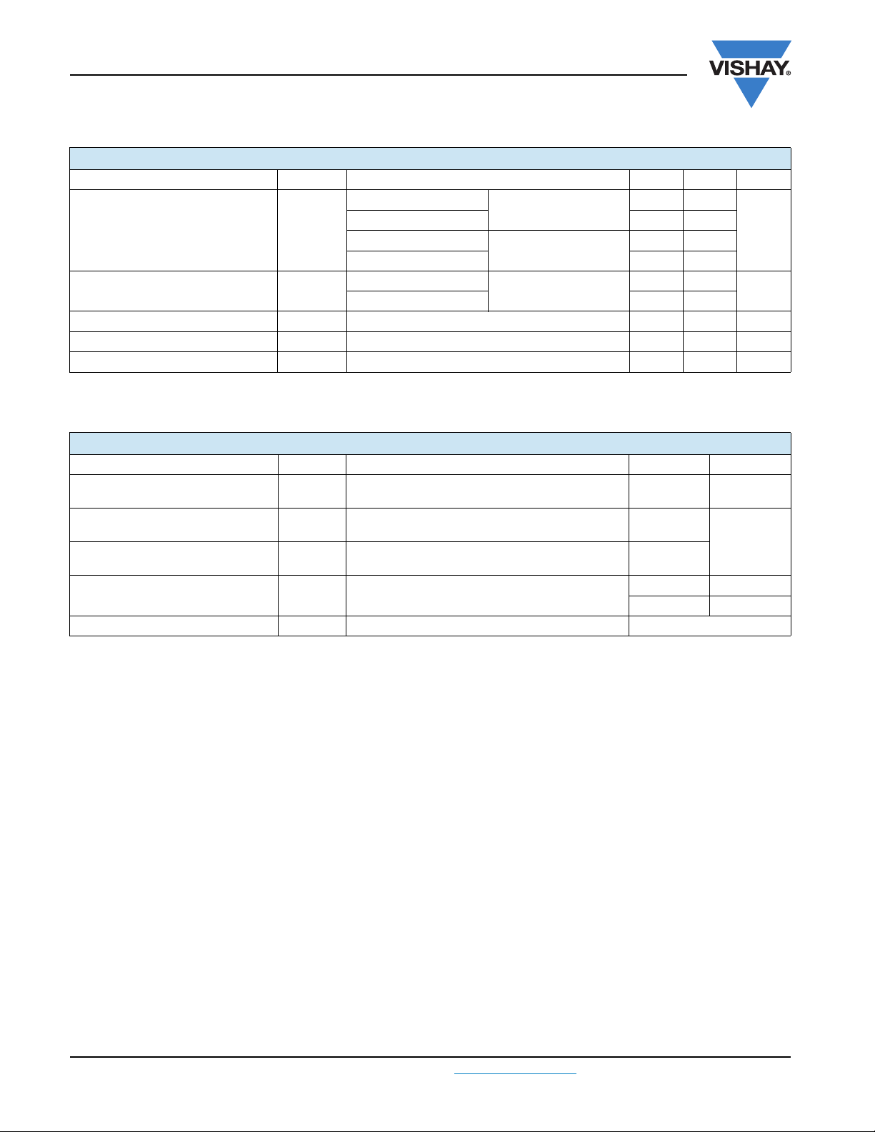
10
TJ = 150 °C
T
T
1.0
- Instantaneous
F
I
Forward Current (A)
0.1
0.2
V
= 125 °C
J
= 25 °C
J
0.4 0.6 0.8 1.0
- Forward Voltage Drop (V)
FM
Schottky Rectifier, 1.0 A
10
1.0
0.1
0.01
- Reverse Current (mA)
0.001
R
I
1.2
0.0001
Vishay High Power Products
TJ = 150 °C
= 125 °C
T
J
= 100 °C
T
J
T
= 75 °C
J
= 50 °C
T
J
T
= 25 °C
J
0
1051520
V
- Reverse Voltage (V)
R
25 30 35
Fig. 1 - Maximum Forward Voltage Drop Characteristics Fig. 2 - Typical Peak Reverse Current vs.
Reverse Voltage
1000
40
100
- Junction Capacitance (pF)
T
C
10
0
TJ = 25 °C
10
V
R
20
- Reverse Voltage (V)
Fig. 3 - Typical Junction Capacitance vs. Reverse Voltage
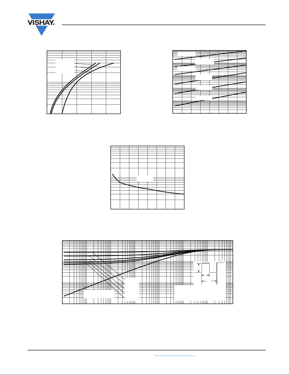
100
10
1
- Thermal Impedance (°C/W)
thJC
Z
0.1
0.00001 0.0001 0.001 0.01 0.1 1
Single pulse
(thermal resistance)
D = 0.75
D = 0.50
D = 0.33
D = 0.25
D = 0.20
t1 - Rectangular Pulse Duration (s)
Fig. 4 - Maximum Thermal Impedance Z
thJC
30
40
P
DM
Notes:
1. Duty factor D = t
2. Peak TJ = PDM x Z
Characteristics (Per Leg)
1/t2
t
1
thJC
10
t
2
.
+ T
C
100
Document Number: 94319 For technical questions, contact: diodestech@vishay.com
www.vishay.com
Revision: 05-Mar-10 3
 Loading...