

Vishay MBRA140TR Data Sheet
Bulletin PD-20582 04/01
MBRA140TR
SCHOTTKY RECTIFIER
Major Ratings and Characteristics
Characteristics MBRA140TR Units
I
Rect. Waveform 1.0 A
FAV
V
RRM
I
@ tp = 5 µs sine 120 A
FSM
VF@ 1.0Apk, TJ=125°C 0.49 V
TJrange - 55 to 150 °C
Device Marking: IR14
40 V
1.0 Amp
SMA
Description/Features
The MBRA140TR surface mount Schottky rectifier has been
designed for applications requiring low forward drop and very
small foot prints on PC boards. Typical applications are in disk
drives, switching power supplies, converters, free-wheeling
diodes, battery charging, and reverse battery protection.
Small foot print, surface mountable
Low forward voltage drop
High frequency operation
Guard ring for enhanced ruggedness and long term
reliability
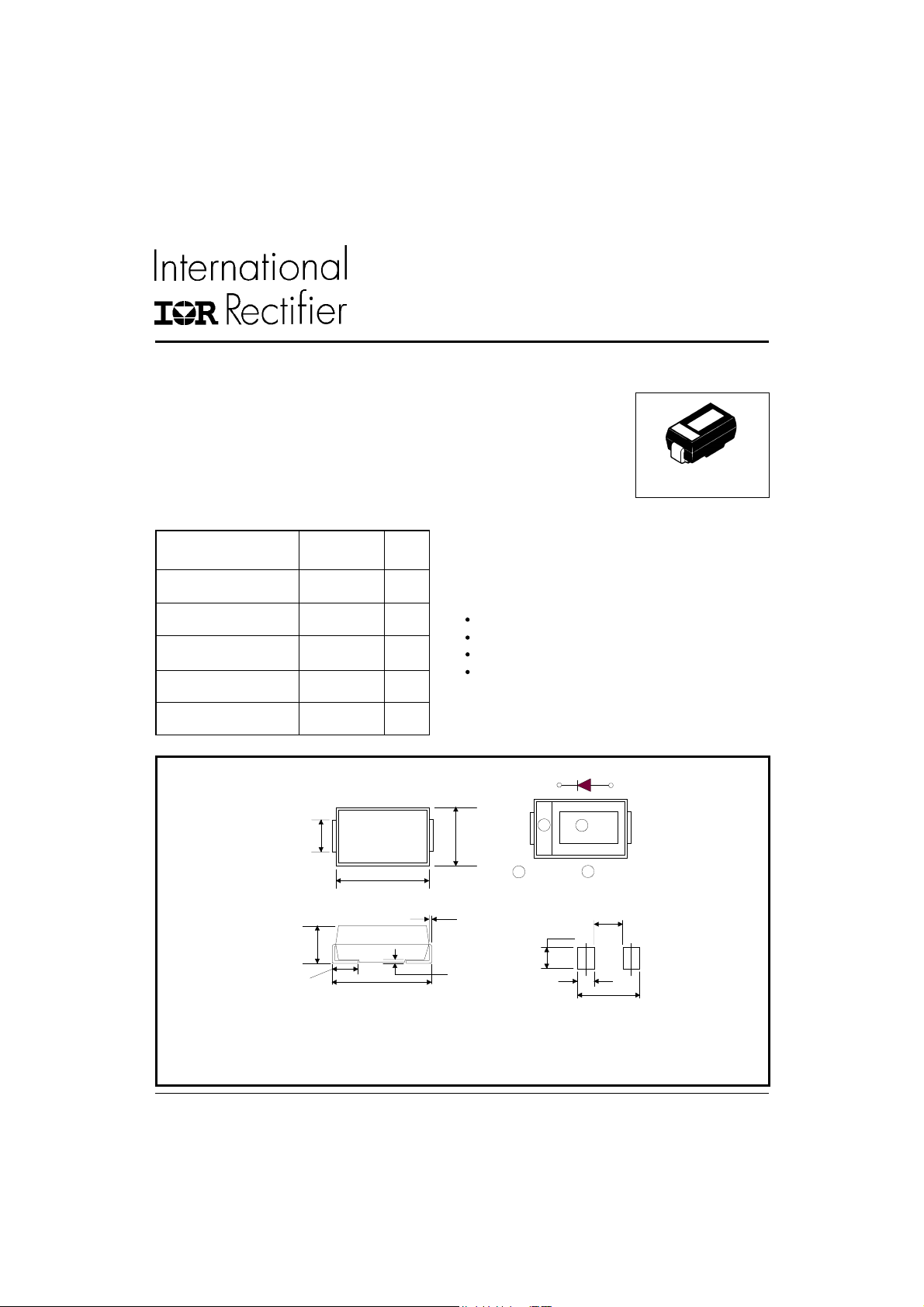
CATHODE ANODE
www.irf.com
1.40 (.055)
1.60 (.062)
2.00 (.078)
2.44 (.096)
0.76 (.030)
1.52 (.060)
4.00 (.157)
4.60 (.181)
4.80 (.188)
5.28 (.208)
2.50 (.098)
2.90 (.114)
.152 (.006)
.305 (.012)
.103 (.004)
.203 (.008)
1 2
1.47 MIN.
SOLDERING PAD
2
2.10 MAX.
(.085 MAX. )
5.53 (.218)
POLARITY PART NUMBER
1
(.058 MIN.)
1.27 MIN.
(.050 MIN.)
Outline SMA Similar to D-64
Dimensions in millimeters and (inches)
For recommended footprint and soldering techniques refer to application note #AN-994
1
MBRA140TR
Bulletin PD-20582 04/01
Voltage Ratings
Part number MBRA140TR
VRMax. DC Reverse Voltage (V)
V
Max. Working Peak Reverse Voltage (V)
RWM
40
Absolute Maximum Ratings
Parameters Value Units Conditions
I
Max. Average Forward Current 1.0 A 50% duty cycle @ TL = 118 °C, rectangular wave form
F(AV)
* See Fig. 4 On PC board 9mm2 island (.013mm thick copper
pad area)
I
Max. Peak One Cycle Non-Repetitive 120 A 5µs Sine or 3µs Rect. pulse
FSM
Surge Current * See Fig. 6 30 10ms Sine or 6ms Rect. pulse
Following any rated
load condition and
with rated V
Electrical Specifications
Parameters Value Units Conditions
VFMMax. Forward Voltage Drop (1) 0.55 V @ 1A
* See Fig. 1 0.71 V @ 2A
0.5 V @ 1A
0.65 V @ 2A
0.49 V @ 1A
0.63 V @ 2A
IRMMax. Reverse Leakage Current (1) 0.5 m A T J = 25 °C
* See Fig. 2 10 mA TJ = 100 °C VR = rated V
26 mA TJ = 125 °C
V
Threshold Voltage 0.36 V TJ = TJ max.
F(TO)
r
Forward Slope Resistance 104 m Ω
t
CTTypical Junction Capacitance 38 pF V R = 10VDC, TJ = 25°C, test signal = 1Mhz
LSTypical Series Inductance 2.0 nH Measured lead to lead 5mm from package body
dv/dt Max. Voltage Rate of Change 10000 V/ µs (Rated VR)
(1) Pulse Width < 300µs, Duty Cycle < 2%
TJ = 25 °C
TJ = 100 °C
TJ = 125 °C
R
RRM
applied
Thermal-Mechanical Specifications
Parameters Value Units Conditions
TJMax. Junction Temperature Range - 55 to 150 °C
T
Max. Storage Temperature Range - 55 to 150 °C
stg
R
Max. Thermal Resistance Junction 35 °C/W D C operation (* See Fig. 4)
thJL
to Lead (2)
wt Approximate Weight 0.07(0.026) g (oz.)
Case Style SMA Similar D-64
(2) Mounted 1 inch square PCB, Thermal Probe connected to lead 2mm from Package
2
www.irf.com
 Loading...