

Page 1
Bulletin PD-2.325 rev. D 07/01
C
Anode
1
3
Base
Cathode
2
N/C
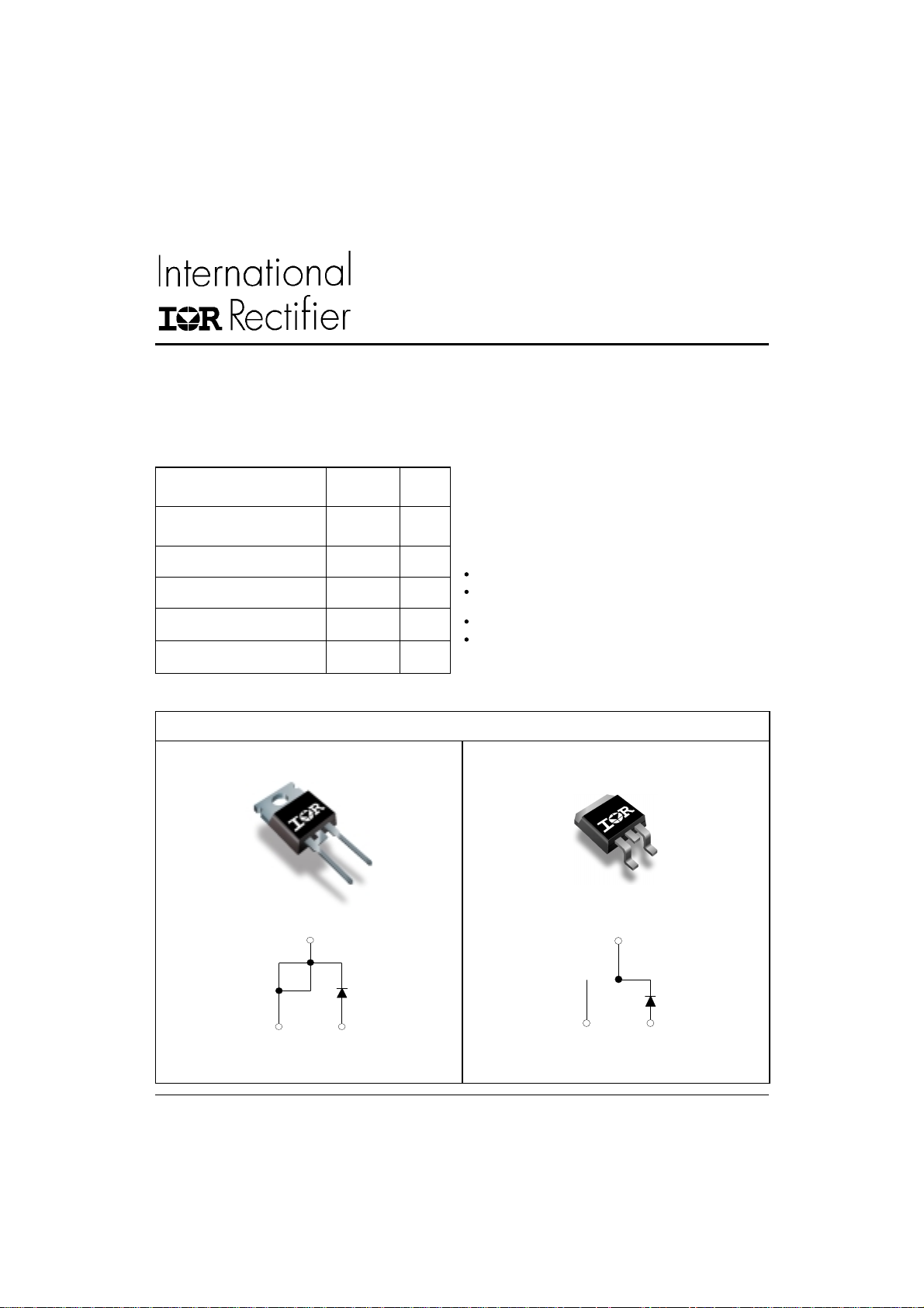
MBR735/ MBR745
MBRB735/ MBRB745
SCHOTTKY RECTIFIER
Major Ratings and Characteristics
Characteristics Values Units
I
Rectangular 7.5 A
F(AV)
waveform
V
RRM
I
@ tp = 5 µs sine 690 A
FSM
V
@ 7.5 Apk, TJ = 125°C 0.57 V
F
T
range - 65 to 150 °C
J
MBR735/ MBR745
35/ 45 V
7.5 Amp
Description/Features
The MBR7.. Schottky rectifier has been optimized for low
reverse leakage at high temperature. The proprietary barrier
technology allows for reliable operation up to 150° C junction
temperature. Typical applications are in switching power
supplies, converters, free-wheeling diodes, and reverse battery
protection.
150° C TJ operation
High purity, high temperature epoxy encapsulation for
enhanced mechanical strength and moisture resistance
High frequency operation
Guard ring for enhanced ruggedness and long term
reliability
Case Styles
MBRB735/ MBRB745
Base
Cathode
1
athode
TO-220AC
www.irf.com
3
Anode
D
2
PAK
1
Page 2
MBR735/ MBR745, MBRB735/ MBRB745
Bulletin PD-2.325 rev. D 07/01
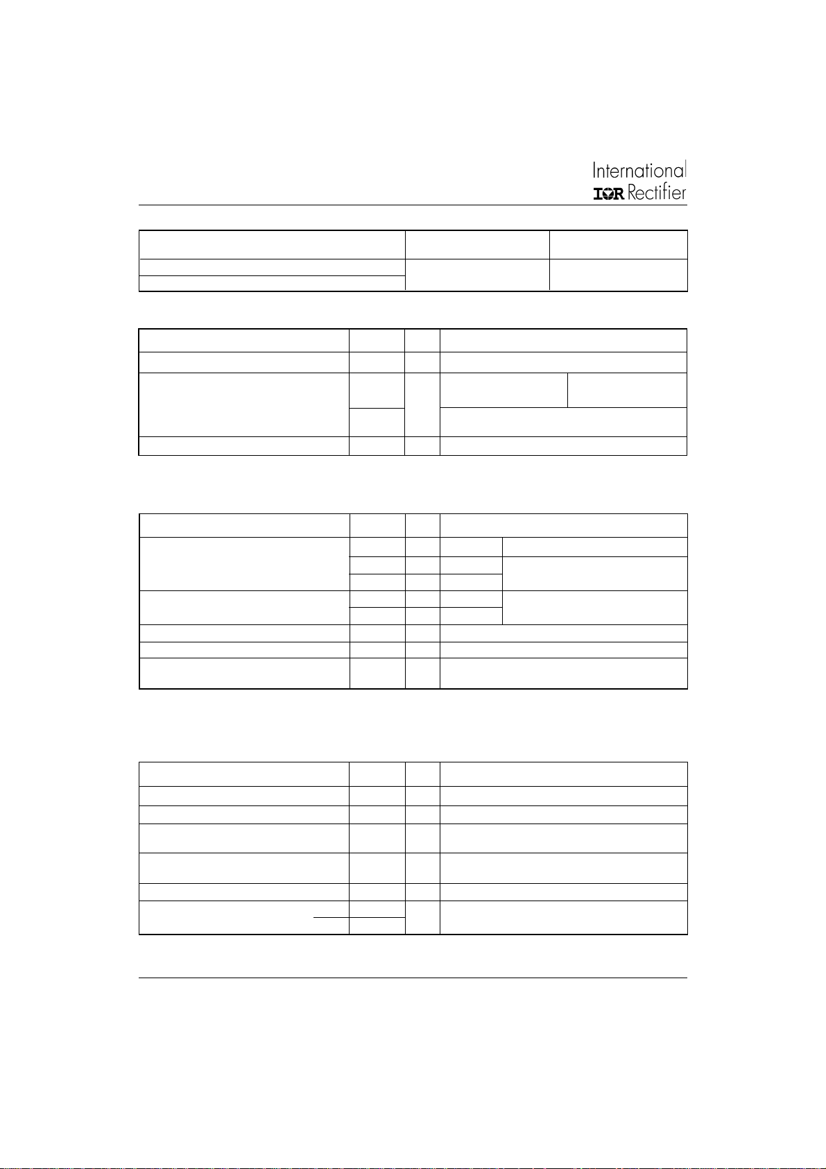
Voltage Ratings
Parameters MBR.735 MBR.745
VRMax. DC Reverse Voltage (V) 35 45
V
Max. Working Peak Reverse Voltage (V)
RWM
Absolute Maximum Ratings
Parameters MBR.. Conditions
I
Max. Average Forward Current 7.5 A @ TC = 131 °C (Rated VR)
F(AV)
I
Non-Repetitive Peak Surge Current 690 A 5µs Sine or 3µs Rect. pulse
FSM
I
Peak Repetitive Reverse Surge Current 1.0 A 2.0 µsec 1.0 KHz
RRM
Units
Following any rated load
condition and with rated
V
applied
RRM
150 Surge applied at rated load condition halfwave single
phase 60Hz
Electrical Specifications
Parameters MBR.. Conditions
VFMMax. Forward Voltage Drop(1) 0.84 V @ 15A TJ = 25 °C
IRMMax. Instantaneus Reverse Current 0.1 mA TJ = 25 °C Rated DC voltage
(1) 15 mA TJ = 125 °C
CTMax. Junction Capacitance 400 pF VR = 5VDC, (test signal range 100Khz to 1Mhz) 25°C
LSTypical Series Inductance 8.0 nH Measured from top of terminal to mounting plane
dv/dt Max. Voltage Rate of Change 1000 V/ µs
(Rated VR)
(1) Pulse Width < 300µs, Duty Cycle <2%
Units
0.57 V @ 7.5A TJ = 125 °C
0.72 V @ 15A
Thermal-Mechanical Specifications
Parameters MBR.. Conditions
TJMax. Junction Temperature Range - 65 to 150 °C
T
Max. Storage Temperature Range - 65 to 17 5 °C
stg
R
Max. Thermal Resistance Junction 3.0 °C/W DC operation
thJC
to Case
R
Typical Thermal Resistance, Case 0.50 °C/W Mounting surface, smooth and greased
thCS
to Heatsink
wt Approximate Weight 2 (0.07) g (oz.)
T Mounting Torque Min. 6 (5)
Max. 12 (10
2
Units
Kg-cm
(Ibf-in)
www.irf.com
Page 3
MBR735/ MBR745, MBRB735/ MBRB745
Bulletin PD-2.325 rev. D 07/01
100
(A)
F
10
Instantaneous Forward Current - I
T = 150˚C
J
T = 125˚C
J
T = 25˚C
J
100
T = 150˚C
10
(mA)
R
0.1
0.01
Reverse Current - I
0.001
0.0001
J
125˚C
1
100˚C
75˚C
50˚C
25˚C
0 5 10 15 20 25 30 35 40 45
Reverse Voltage - VR (V)
Fig. 2 - Typical Values Of Reverse Current
Vs. Reverse Voltage (Per Leg)
1000
T = 25˚C
(p F)
T
J
1
www.irf.com
Junction Capacitance - C
100
0 0.2 0.4 0.6 0.8 1 1.2 1.4 1.6 1.8 2
Forward Voltage Drop - VFM (V)
Fig. 1 - Max. Forward Voltage Drop Characteristics
(Per Leg)
0 1020304050
Reverse Voltage - VR (V)
Fig. 3 - Typical Junction Capacitance
Vs. Reverse Voltage (Per Leg)
10
D = 0.75
D = 0.50
D = 0.33
1
(°C/W)
thJC
Thermal Impedance Z
0.1
0.01
D = 0.25
D = 0.20
Single Pulse
(Thermal Resistance)
P
DM
Notes:
1. Duty factor D = t1/ t2
2. Peak Tj = Pdm x ZthJC + Tc
0.001
0.00001 0.0001 0.001 0.01 0.1 1 10
t1 , Rectangular Pulse Duration (Seconds)
Fig. 4 - Max. Thermal Impedance Z
Characteristics (Per Leg)
thJC
t
1
t
2
3
Page 4

MBR735/ MBR745, MBRB735/ MBRB745
Bulletin PD-2.325 rev. D 07/01
150
140
130
Square Wave (D = 0.50)
Rated Vr Applied
Allowable Case Temperature (°C)
see note (2)
DC
120
024681012
Average Forward Current - I
Fig. 5 - Max. Allowable Case Temperature
Vs. Average Forward Current
1000
(A)
FSM
Average Power Loss (Watts)
(A)
F(AV)
At Any Rated Load Condition
And With Rated Vrrm Applied
Following Surge
7
D = 0.75
D = 0.50
6
D = 0.33
D = 0.25
5
D = 0.20
4
RMS Limit
3
DC
2
1
0
024681012
Average Forward Current - I
F(AV)
(A)
Fig. 6 - Forward Power Loss Characteristics
(2) Formula used: TC = TJ - (Pd + Pd
Pd = Forward Power Loss = I
Pd
= Inverse Power Loss = VR1 x IR (1 - D); IR @ V
REV
F(AV)
4
Non-Repetitive Surge Current - I
100
10 100 1000 10000
Square Wave Pulse Duration - tp (microsec)
Fig. 7 - Max. Non-Repetitive Surge Current (Per Leg)
) x R
thJC
;
F(AV)
/ D) (see Fig. 6);
= rated V
R1
R
REV
x VFM @ (I
www.irf.com
Page 5

Outline Table
Anode
1
3
Base
Cathode
Cathode
N
MBR735/ MBR745, MBRB735/ MBRB745
Bulletin PD-2.325 rev. D 07/01
10.54 (0.41)
15.24 (0.60)
14.84 (0.58)
14.09 (0.55)
13.47 (0.53)
4.57 (0.18)
4.32 (0.17)
MAX.
1
1.40 (0.05)
1.15 (0.04)
1
TERM 2
3
2.04 (0.080) MAX.
0.94 (0.04)
0.69 (0.03)
3
5.08 (0.20) REF.
3.78 (0.15)
3.54 (0.14)
2.92 (0.11)
2.54 (0.10)
3.96 (0.16)
3.55 (0.14)
0.61 (0.02) MAX.
DIA.
Conform to JEDEC outline TO-220AC
Dimensions in millimeters and (inches)
10.16 (0.40)
REF.
1.40 (0.055)
3X
1.14 (0.045)
93°
8.89 (0.35)
13
2
REF.
2X
5.08 (0.20) REF.
/C
Base
Cathode
1
15.49 (0.61)
14.73 (0.58)
2
3
Anode
Conform to JEDEC outline D2Pak (SMD-220)
Dimensions in millimeters and (inches)
6.48 (0.25)
6.23 (0.24)
2.61 (0.10)
2.32 (0.09)
0.93 (0.37)
0.69 (0.27)
4.57 (0.18)
4.32 (0.17)
6.47 (0.25)
6.18 (0.24)
0.61 (0.02) MAX.
1.32 (0.05)
1.22 (0.05)
2°
0.10 (0.004)
2.89 (0.11)
2.64 (0.10)
4.69 (0.18)
4.20 (0.16)
1.32 (0.05)
1.22 (0.05)
5.28 (0.21)
4.78 (0.19)
0.55 (0.02)
0.46 (0.02)
MINIMUM RECOMMENDED FOOTPRINT
11.43 (0.45)
8.89 (0.35)
3.81 (0.15)
2.08 (0.08)
2X
17.78 (0.70)
2.54 (0.10)
2X
www.irf.com
5
Page 6

MBR735/ MBR745, MBRB735/ MBRB745
Bulletin PD-2.325 rev. D 07/01
Tape & Reel Information
TRR
1.60 (0.063)
1.50 (0.059)
4.10 (0.161)
3.90 (0.153)
FEED DIRECTION
TRL
FEED DIRECTION
1.85 (0.07 3)
1.65 (0.06 5)
10.90 (0.429)
10.70 (0.421)
1.60 (0.063)
1.50 (0.059)
11.60 (0.457)
11.40 (0.449)
1.75 (0.069)
1.25 (0.049)
16.10 (0.6 34)
15.90 (0.6 26)
DIA.
DIA.
15.42 (0.609)
15.22 (0.601)
0.368 (0.014 5)
0.342 (0.013 5)
24 .30 (0 .957 )
23 .90 (0 .941 )
4.72 (0.18 6)
4.52 (0.17 8)
13.50 ( 0.532)
12.80 ( 0.504)
360 (14.173)
DIA. MAX.
Ordering Information Table
Device Code
1 - Essential Part Number
2 - Package Style: none = TO-220
3 - Current Rating
4 - Voltage Rating
DIA.
MBR B 7 45
1 2 3
B= D2 Pak
26.40 (1.039)
24.40 (0.961)
60 (2.36 2)
4
SMD-220 Tape & Reel
When ordering, indi cate the part
number, part orientation, and t he
quantity. Quantities are in multiples
of 8 00 p iece s pe r reel for b oth
DIA. MIN.
TRL a nd TRR.
Dimensions in millimeters and (inches)
35 = 35V
45 = 45V
6
www.irf.com
Page 7

MBR735/ MBR745, MBRB735/ MBRB745
Bulletin PD-2.325 rev. D 07/01
MBR745
********************************************
* This model has been developed by *
* Wizard SPICE MODEL GENERATOR (1999) *
* (International Rectifier Corporation) *
* contains Proprietary Information *
********************************************
* SPICE Model Diode is composed by a *
* simple diode plus paralled VCG2T *
********************************************
.SUBCKT MBR745 ANO CAT
D1 ANO 1 DMOD (0.03191)
*Define diode model
.MODEL DMOD D(IS=9.72464638473799E-05A,N=1.30648926537753,BV=52V,
+ IBV=0.195508065728349A,RS= 0.000727548,CJO=1.94829876431799E-08,
+ VJ=2.27282978121533,XTI=2, EG=0.854458710837653)
********************************************
*Implementation of VCG2T
VX 1 2 DC 0V
R1 2 CAT TRES 1E-6
.MODEL TRES RES(R=1,TC1=27.6281424524011)
GP1 ANO CAT VALUE={-ABS(I(VX))*(EXP((((-5.219758E-03/27.62814)*((V(2,CAT)*1E6)/(I(VX)+1E-6)-
1))+1)*7.000165E-02*ABS(V(ANO,CAT)))-1)}
********************************************
.ENDS MBR745
Thermal Model Subcircuit
.SUBCKT MBR745 5 1
CTHERM1 5 4 1.05E+00
CTHERM2 4 3 4.44E+00
CTHERM3 3 2 1.16E+01
CTHERM4 2 1 6.12E+01
RTHERM1 5 4 1.33E+00
RTHERM2 4 3 1.19E+00
RTHERM1 3 2 3.81E-01
RTHERM1 2 1 9.54E-02
.ENDS MBR745
Data and specifications subject to change without notice.
This product has been designed and qualified for Industrial Level.
Qualification Standards can be found on IR's Web site.
IR WORLD HEADQUARTERS: 233 Kansas St., El Segundo, California 90245, USA Tel: (310) 252-7105
TAC Fax: (310) 252-7309
Visit us at www.irf.com for sales contact information. 07/01
www.irf.com
7
 Loading...