

Page 1
Bulletin PD-20715 rev. A 09/00
MBR4045WT
SCHOTTKY RECTIFIER 40 Amp
I
= 40Amp
F(AV)
VR = 45V
Major Ratings and Characteristics
Characteristics Values Units
I
Rectangular waveform 40 A
F(AV)
(Per Device)
I
@ TC = 125°C 40 A
FRM
(Per Leg)
V
RRM
I
@ tp = 5 µs sine 1020 A
FSM
VF@ 20 Apk, TJ = 125°C 0.56 V
TJrange - 55 to 15 0 °C
45 V
Description/Features
The MBR4045WT center tap Schottky rectifier has been optimized for very low forward voltage drop, with moderate leakage.
The proprietary barrier technology allows for reliable operation
up to 150° C junction temperature. Typical applications are in
switching power supplies, converters, free-wheeling diodes,
and reverse battery protection.
150° C TJ operation
Center tap TO-247 package
High purity, high temperature epoxy encapsulation for
enhanced mechanical strength and moisture resistance
Very low forward voltage drop
High frequency operation
Guard ring for enhanced ruggedness and long term
reliability
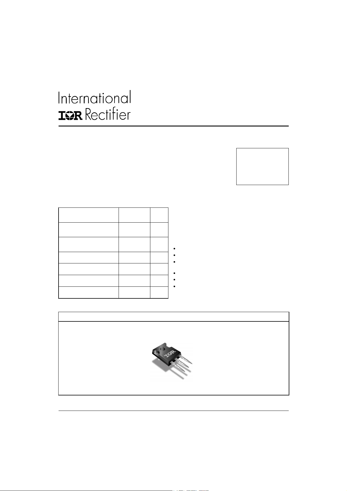
Case Styles
MBR4045WT
TO-247AC
1www.irf.com
Page 2
MBR4045WT
Bulletin PD-20715 rev. A 09/00
Voltage Ratings
Part number MBR4045WT
VRMax. DC Reverse Voltage (V)
V
Max. Working Peak Reverse Voltage (V)
RWM
45
Absolute Maximum Ratings
Parameters Values Units Conditions
I
Max. Average Forward (Per Leg) 20 @ TC = 125°C, 50% duty cycle, rectangular waveform
F(AV)
Current (Per Device) 40
I
Peak Repetitive Forward 40 A Rated VR , square wave, 20kHz
FRM
Current (Per Leg) TC = 125° C
I
Max.Peak One Cycle Non-Repetitive 1020 5µs Sine or 3µs Rect. pulse
FSM
Surge Current ( Per Leg) See fig.7 265 10ms Sine or 6ms Rect. pulse
EASNon-Repetitive Avalanche Energy 20 mJ TJ = 25 °C, I
(Per Leg)
IARRepetitive Avalanche Current 3 A Current decaying linearly to zero in 1 µsec
(Per Leg) Frequency limited by T
A
Following any rated
A
= 3 Amps, L = 4.40 mH
AS
load condition and with
rated V
max. VA = 1.5 x VR typical
J
RRM
applied
Electrical Specifications
Parameters Values Units Conditions
VFMMax. Forward Voltage Drop 0.59 V @ 20A
0.78 V @ 40A
(1) 0.56 V @ 20A
0.72 V @ 40A
IRMMax. Instantaneus Reverse Current 1.75 m A TJ = 25 °C
(1) 50 m A TJ = 100 °C
85 mA TJ = 125 °C
V
Threshold Voltage 0.29 V TJ = TJ max.
F(TO)
r
Forward Slope Resistance 10.3 mΩ
t
CTMax. Junction Capacitance 900 pF VR = 5VDC (test signal range 100Khz to 1Mhz) 25°C
LSTypical Series Inductance 7.5 nH Measured from top of terminal to mounting plane
dv/dt Max. Voltage Rate of Change 10000 V/ µs
(Rated VR)
Thermal-Mechanical Specifications
Parameters Values Units Conditions
TJMax. Junction Temperature Range -55 to 150 °C
T
Max. Storage Temperature Range -55 to 175 °C
stg
R
Max. Thermal Resistance 1.4 °C/W DC operation
thJC
Junction to Case (Per Package)
R
Typical Thermal Resistance 0.7 °C/W Mounting surface, smooth and greased
thCS
Case to Heatsink
wt Approximate Weight 6 (0.21) g (oz.)
T Mounting Torque Min. 6 (5)
Max. 12 (10)
Case Style TO-247AC (TO-3P) JEDEC
Kg-cm
(Ibf-in)
TJ = 25 °C
TJ = 125 °C
Rated DC voltage
(1) Pulse Width < 300µs, Duty Cycle <2%
2
www.irf.com
Page 3

MBR4045WT
0
0
Bulletin PD-20715 rev. A 09/00
1000
100
(A)
F
10
Instantaneous Forward Current - I
T = 150˚C
J
T = 125˚C
J
T = 25˚C
J
1000
T = 150˚C
10
J
125˚C
1
100˚C
(mA)
R
100
75˚C
0.1
Reverse Current - I
0.01
.001
0 1020304050
50˚C
25˚C
Reverse Voltage - VR (V)
Fig. 2 - Typical Values Of Reverse Current
Vs. Reverse Voltage
1000
(pF)
T
T = 25˚C
J
1
0 0.4 0.8 1.2 1.6 2
Forward Voltage Drop - VFM (V)
Fig. 1 - Max. Forward Voltage Drop Characteristics
10
(°C/W)
thJC
D = 0.75
1
D = 0.50
D = 0.33
D = 0.25
D = 0.20
0.1
Single Pulse
Thermal Impedance Z
.01
0.00001 0.0001 0.001 0.01 0.1 1 1 0 100
(Thermal Resistance)
t 1, Rectangular Pulse Duration (Seconds)
Fig. 4 - Max. Thermal Impedance Z
www.irf.com
Junction Capacitance - C
100
0 1020304050
Fig. 3 - Typical Junction Capacitance
P
DM
Notes:
1. Duty factor D = t / t
2. Peak T = P x Z + T
J
DM
Characteristics
thJC
Reverse Voltage - VR (V)
Vs. Reverse Voltage
t
1
t
2
1
2
C
thJC
3
Page 4

MBR4045WT
1
1
2
Bulletin PD-20715 rev. A 09/00
160
140
DC
120
Square wave (D = 0.50)
Rated V applied
R
100
Allowable Case Temperature (°C)
see note (2)
80
0 5 10 15 20 25 30
Average Forward Current - I
(AV)
F
Fig. 5 - Max. Allowable Case Temperature
Vs. Average Forward Current
1000
(A)
FSM
Non-Repetitive Surge Current - I
100
10 100 1000 10000
Square Wave Pulse Duration - t
Fig. 7 - Max. Non-Repetitive Surge Current
Average Power Loss (Watts)
(A)
Fig. 6 - Forward Power Loss Characteristics
At Any Rated Load Condition
And With Rated V Applied
Following Surge
RRM
(microsec)
p
0
D = 0.20
D = 0.25
D = 0.33
5
D = 0.50
D = 0.75
0
RMS Limit
DC
5
0
0 5 10 15 20 25 30
Average Forward Current - I
(A)
(AV)
F
L
HIGH-SPEED
SW ITCH
FREE-WHEEL
D IO D E
40HFL40S02
Vd = 25 Volt
+
CURRENT
MONITOR
DUT
IRFP460
Rg = 25 ohm
Fig. 8 - Unclamped Inductive Test Circuit
(2) Formula used: TC = TJ - (Pd + Pd
Pd = Forward Power Loss = I
Pd
= Inverse Power Loss = VR1 x IR (1 - D); IR @ V
REV
4
REV
x VFM @ (I
F(AV)
) x R
;
thJC
/ D) (see Fig. 6);
F(AV)
= rated V
R1
R
www.irf.com
Page 5

Outline Table
)
MBR4045WT
Bulletin PD-20715 rev. A 09/00
15.90 (0.626)
15.30 (0.602)
20.30 (0.800)
19.70 (0.775)
1 2 3
14.80 (0.583)
14.20 (0.559)
1.40 (0.056)
1.00 (0.039)
5.47 (0.216)
5.43 (0.213)
Conform to JEDEC outline TO-247AC (TO-3P)
Ordering Information Table
3.65 (0.144)
3.55 (0.139)
DIA.
5.30 (0.209)
4.70 (0.185)
5.70 (0.225)
5.30 (0.208)
5.50 (0.217)
4.50 (0.177)
(2 PLCS.)
4.30 (0.170)
3.70 (0.145)
2.20 (0.087)
MAX.
3.20 (0.126)
MAX.
0.80 (0.032)
0.40 (0.213)
Dimensions in millimeters and (inches)
2.5 (0.098)
1.5 (0.059)
2.40 (0.095
MAX.
BASE
COMMON
CATHODE
2
123
ANODEANODE
COMMON
CATHODE
www.irf.com
Device Code
1 - Schottky MBR Series
2 - Currrent Rating : 40 = 40A
3 - Voltage Rating : 45 = 45V
4 - Circuit Configuration :
MBR 40 45 WT
1
2
Center Tap (Dual) TO-247
4
3
5
Page 6

MBR4045WT
Bulletin PD-20715 rev. A 09/00
MBR4045WT
********************************************
This model has been developed by
Wizard SPICE MODEL GENERATOR (1999)
(International Rectifier Corporation)
contains Proprietary Information
********************************************
SPICE Model Diode is composed by a
simple diode plus paralled VCG2T
********************************************
.SUBCKT MBR4045WT ANO CAT
D1 ANO 1 DMOD (0.07089)
*Define diode model
.MODEL DMOD D(IS=1.87674447387184E-04A,N=1.0815129563336,BV=51V,
+ IBV=0.370052071012812A,RS= 0.000482052,CJO=1.77083341686508E-08,
+ VJ=2.63120433908928,XTI=2, EG=0.680665296447736)
********************************************
*Implementation of VCG2T
VX 1 2 DC 0V
R1 2 CAT TRES 1E-6
.MODEL TRES RES(R=1,TC1=30.266567848718)
GP1 ANO CAT VALUE={-ABS(I(VX))*(EXP((((-2.374754E-03/30.26657)*((V(2,CAT)*1E6)/(I(VX)+1E-6)-
1))+1)*6.049001E-02*ABS(V(ANO,CAT)))-1)}
********************************************
.ENDS MBR4045WT
Thermal Model Subcircuit
.SUBCKT MBR4045WT 5 1
CTHERM1 5 4 8.75E-01
CTHERM2 4 3 1.19E+01
CTHERM3 3 2 7.69E+01
CTHERM4 2 1 4.98E+02
RTHERM1 5 4 1.00E-04
RTHERM2 4 3 7.15E-01
RTHERM1 3 2 5.30E-01
RTHERM1 2 1 1.50E-01
.ENDS MBR4045WT
WORLD HEADQUARTERS: 233 Kansas St., El Segundo, California 90245 U.S.A. Tel: (310) 322 3331. Fax: (310) 322 3332.
EUROPEAN HEADQUARTERS: Hurst Green, Oxted, Surrey RH8 9BB, U.K. Tel: ++ 44 1883 732020. Fax: ++ 44 1883 733408.
IR SOUTHEAST ASIA: 1 Kim Seng Promenade, Great World City West Tower,13-11, Singapore 237994. Tel: ++ 65 838 4630.
http://www.irf.com Fax-On-Demand: +44 1883 733420 Data and specifications subject to change without notice.
IR CANADA: 15 Lincoln Court, Brampton, Markham, Ontario L6T3Z2. Tel: (905) 453 2200. Fax: (905) 475 8801.
IR GERMANY: Saalburgstrasse 157, 61350 Bad Homburg. Tel: ++ 49 6172 96590. Fax: ++ 49 6172 965933.
IR ITALY: Via Liguria 49, 10071 Borgaro, Torino. Tel: ++ 39 11 4510111. Fax: ++ 39 11 4510220.
IR FAR EAST: K&H Bldg., 2F, 30-4 Nishi-Ikebukuro 3-Chome, Toshima-Ku, Tokyo, Japan 171. Tel: 81 3 3983 0086.
IR TAIWAN: 16 Fl. Suite D.207, Sec. 2, Tun Haw South Road, Taipei, 10673, Taiwan. Tel: 886 2 2377 9936.
6
www.irf.com
 Loading...