

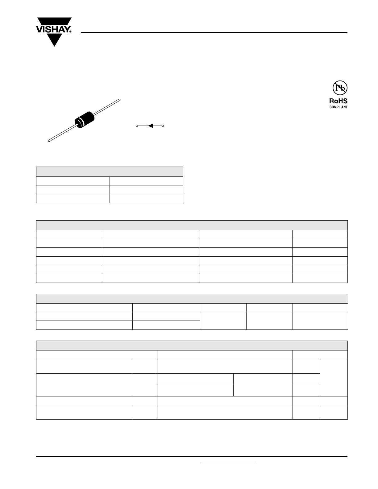
DO-204AL
Schottky Rectifier, 1 A
FEATURES
• Low profile, axial leaded outline
• Very low forward voltage drop
• High frequency operation
Cathode Anode
• High purity, high temperature epoxy encapsulation for
enhanced mechanical strength and moisture resistance
• Guard ring for enhanced ruggedness and long term
reliability
• Lead (Pb)-free plating
• Designed and qualified for industrial level
MBR150, MBR160
Vishay High Power Products
PRODUCT SUMMARY
I
F(AV)
V
R
I
RM
1 A
50/60 V
10 mA at 125 °C
DESCRIPTION
The MBR150, MBR160 axial leaded Schottky rectifier has
been optimized for very low forward voltage drop, with
moderate leakage. Typical applications are in switching
power supplies, converters, freewheeling diodes, and
reverse battery protection.
MAJOR RATINGS AND CHARACTERISTICS
SYMBOL CHARACTERISTICS VALUES UNITS
I
F(AV)
V
RRM
I
FSM
V
F
T
J
Rectangular waveform 1.0 A
50/60 V
tp = 5 µs sine 150 A
1 Apk, TJ = 125 °C 0.65 V
Range - 40 to 150 °C
VOLTAGE RATINGS
PARAMETER SYMBOL MBR150 MBR160 UNITS
Maximum DC reverse voltage V
Maximum working peak reverse voltage V
R
RWM
50 60 V
ABSOLUTE MAXIMUM RATINGS
PARAMETER SYMBOL TEST CONDITIONS VALUES UNITS
Maximum average forward current
See fig. 4
Maximum peak one cycle
non-repetitive surge current
See fig. 6
Non-repetitive avalanche energy E
Repetitive avalanche current I
I
F(AV)
I
FSM
AR
50 % duty cycle at TC = 75 °C, rectangular waveform 1.0
5 µs sine or 3 µs rect. pulse
10 ms sine or 6 ms rect. pulse 25
TJ = 25 °C, I
AS
Current decaying linearly to zero in 1 µs
Frequency limited by, T
= 1 A, L = 4 mH 2.0 mJ
AS
maximum VA = 1.5 x VR typical
J
Following any rated load
condition and with rated
V
applied
RRM
150
1.0 A
A
Document Number: 93439 For technical questions, contact: diodes-tech@vishay.com
Revision: 06-Nov-08 1
www.vishay.com
MBR150, MBR160
Vishay High Power Products
Schottky Rectifier, 1 A
ELECTRICAL SPECIFICATIONS
PARAMETER SYMBOL TEST CONDITIONS VALUES UNITS
1 A
2 A 0.9
Maximum forward voltage drop
See fig. 1
V
FM
3 A 1.0
(1)
1 A
2 A 0.75
3 A 0.82
TJ = 25 °C
Maximum reverse leakage current
See fig. 2
Typical junction capacitance C
Typical series inductance L
(1)
I
RM
T
S
J
T
J
VR = 5 VDC (test signal range 100 kHz to 1 MHz) 25 °C 55 pF
Measured lead to lead 5 mm from package body 8.0 nH
Maximum voltage rate of change dV/dt Rated V
Note
(1)
Pulse width < 300 µs, duty cycle < 2 %
T
= 25 °C
J
T
= 125 °C
J
= 100 °C 5
= Rated V
V
R
R
= 125 °C 10
R
0.75
0.65
0.5
10 000 V/µs
V
mAT
THERMAL - MECHANICAL SPECIFICATIONS
PARAMETER SYMBOL TEST CONDITIONS VALUES UNITS
Maximum junction and storage
temperature range
Maximum thermal resistance,
junction to lead
Approximate weight
Marking device Case style DO-204AL (DO-41)
Notes
dP
(1)
------------dT
(2)
Mounted 1" square PCB, thermal probe connected to lead 2 mm from package
1
tot
J
thermal runaway condition for a diode on its own heatsink
--------------<
R
thJA
(1)
T
, T
J
Stg
DC operation
(2)
R
thJL
See fig. 4
- 40 to 150 °C
80 °C/W
0.33 g
0.012 oz.
MBR150
MBR160
www.vishay.com For technical questions, contact: diodes-tech@vishay.com
Document Number: 93439
2 Revision: 06-Nov-08

MBR150, MBR160
Schottky Rectifier, 1 A
10
(A)
F
1
Instantaneous Forward Current - I
Tj = 150˚C
Tj = 125˚C
Tj = 25˚C
0.1
0 0.2 0.4 0.6 0.8 1 1.2 1.4 1.6
Forward Voltage Drop - VFM (V)
Fig. 1 - Maximum Forward Voltage Drop Characteristics
Vishay High Power Products
100
(pF)
T
Junction Capacitance - C
10
0 10203040506070
Fig. 3 - Typical Junction Capacitance vs. Reverse Voltage
160
140
120
100
80
60
Square wave (D = 0.50)
40
80% Rated Vr applied
20
Allowable Lead Temperature (°C)
see note (1)
0
0 0.2 0.4 0.6 0.8 1 1.2 1.4 1.6
Average Forward Current - I
Fig. 4 - Maximum Ambient Temperature vs.
Average Forward Current, Printed Circuit Board Mounted
T = 25˚C
J
Reverse Voltage - VR (V)
DC
F(AV)
(A)
100
T = 150˚C
J
125˚C
(mA)
R
10
1
0.1
0.01
Reverse Current - I
0.001
25˚C
0.0001
0 10203040506070
Reverse Voltage - VR(V)
Fig. 2 - Typical Values of Reverse Current vs.
1
0.8
0.6
RMS Limit
0.4
D = 0.20
D = 0.25
D = 0.33
D = 0.50
D = 0.75
0.2
Average Power Loss (Watts)
0
0 0.2 0.4 0.6 0.8 1 1.2 1.4 1.6
Average Forward Current - I
DC
Fig. 5 - Forward Power Loss Characteristics
F(AV)
(A)
Reverse Voltage
Note
(1)
Formula used: TC = TJ - (Pd + Pd
Pd = Forward power loss = I
F(AV)
) x R
REV
x VFM at (I
;
thJC
/D) (see fig. 6); Pd
F(AV)
= Inverse power loss = VR1 x IR (1 - D); IR at VR1 = 80 % rated V
REV
R
Document Number: 93439 For technical questions, contact: diodes-tech@vishay.com
www.vishay.com
Revision: 06-Nov-08 3
MBR150, MBR160
Vishay High Power Products
1000
)A
(
M
SF
I
-
t
n
e
r
r
uC egruS
e
vi
ti
t
ep
eR
noN
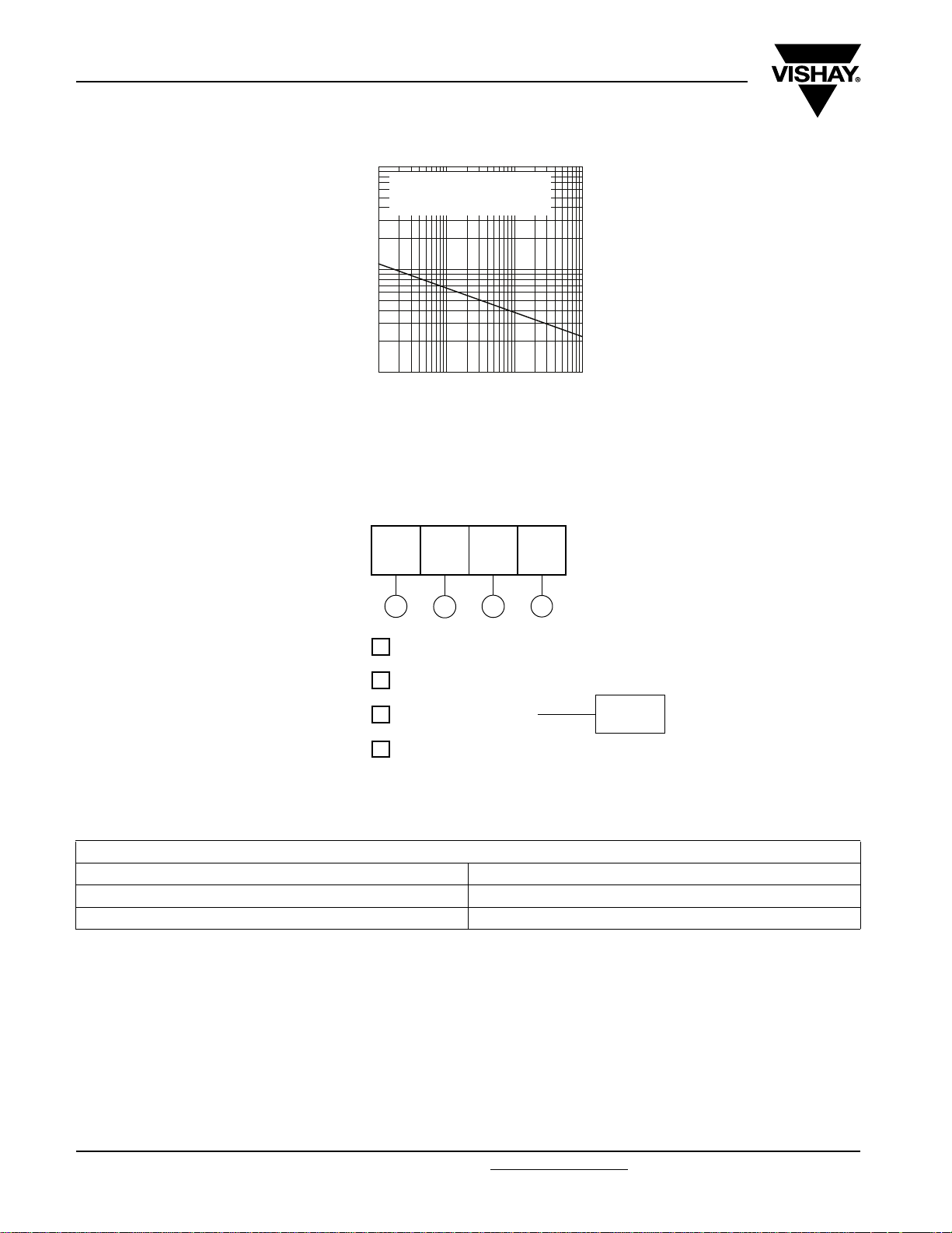
ORDERING INFORMATION TABLE
Schottky Rectifier, 1 A
At Any Rated Load Condition
And With Rated Vrrm Applied
Following Surge
100
10
10 100 1000 10000
Square Wave Pulse Duration - t p (microsec)
Fig. 6 - Maximum Non-Repetitive Surge Current
Device code
MBR 1 60 TR
1324
1 - Schottky MBR series
2 - Current rating: 1 = 1 A
3 - Voltage rating
50 = 50 V
60 = 60 V
4 - TR = Tape and reel package (5000 pcs)
None = Box package (1000 pcs)
LINKS TO RELATED DOCUMENTS
Dimensions http://www.vishay.com/doc?95241
Part marking information http://www.vishay.com/doc?95304
Packaging information http://www.vishay.com/doc?95308
www.vishay.com For technical questions, contact: diodes-tech@vishay.com
4 Revision: 06-Nov-08
Document Number: 93439
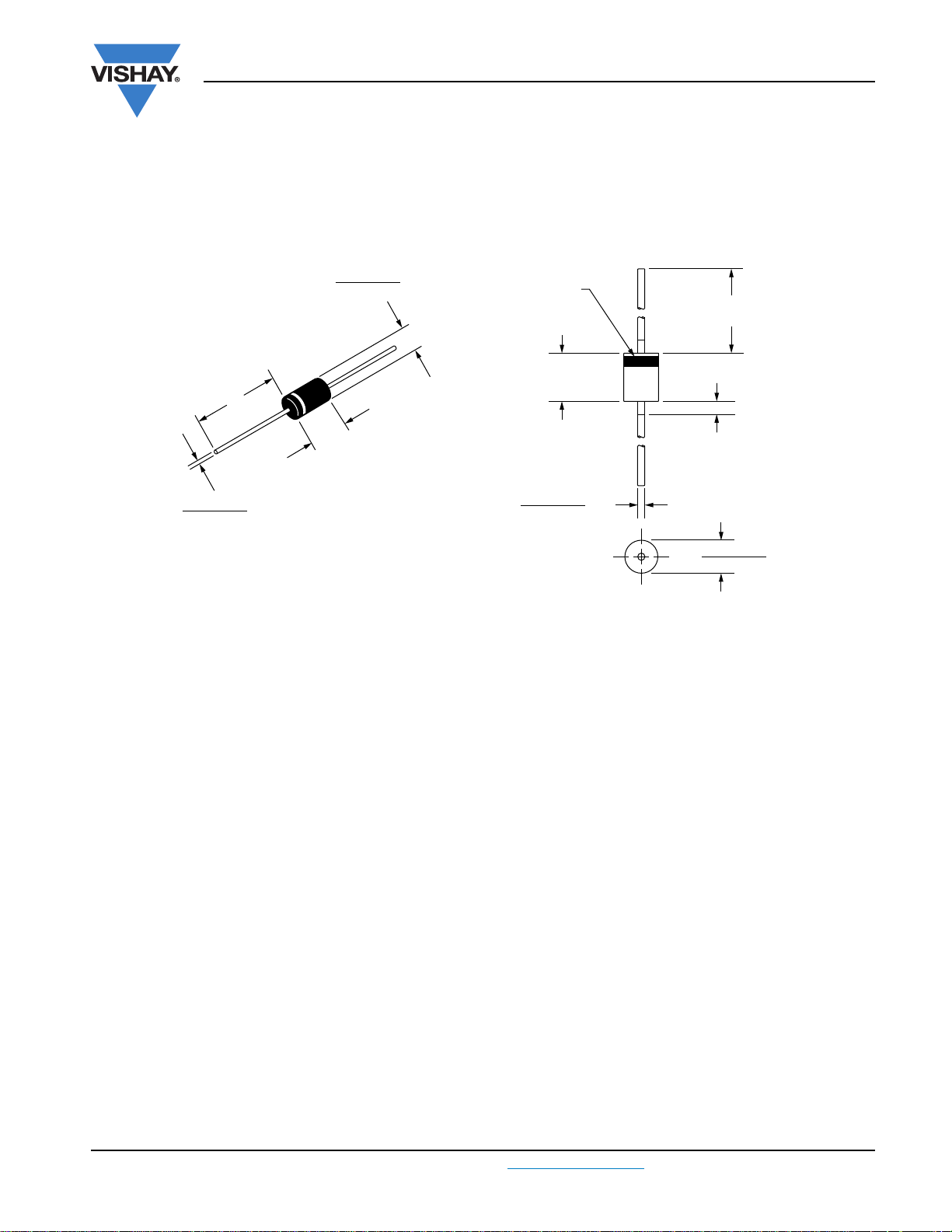
DIMENSIONS in millimeters (inches)
2.70 (0.106)
2.29 (0.090)
DIA.
2.70 (0.106)
2.29 (0.090)
DIA.
0.86 (0.034)
0.72 (0.028)
(2 places)
27.0 (1.06) MIN.
(2 places)
5.21 (0.205)
MAX.
5.21 (0.205)
MAX.
27.0 (1.06) MIN.
(2 places)
1.27 (0.050) MAX.
Flash (2 places)
DIA.
0.86 (0.034)
0.72 (0.028)
(2 places)
DIA.
Cathode band
Outline Dimensions
Vishay Semiconductors
Axial DO-204AL (DO-41)
Document Number: 95241 For technical questions, contact: indmodules@vishay.com
Revision: 22-Nov-07 1
www.vishay.com

Legal Disclaimer Notice
Vishay
Disclaimer
ALL PRODUCT, PRODUCT SPECIFICATIONS AND DATA ARE SUBJECT TO CHANGE WITHOUT NOTICE TO IMPROVE
RELIABILITY, FUNCTION OR DESIGN OR OTHERWISE.
Vishay Intertechnology, Inc., its affiliates, agents, and employees, and all persons acting on its or their behalf (collectively,
“Vishay”), disclaim any and all liability for any errors, inaccuracies or incompleteness contained in any datasheet or in any other
disclosure relating to any product.
Vishay makes no warranty, representation or guarantee regarding the suitability of the products for any particular purpose or
the continuing production of any product. To the maximum extent permitted by applicable law, Vishay disclaims (i) any and all
liability arising out of the application or use of any product, (ii) any and all liability, including without limitation special,
consequential or incidental damages, and (iii) any and all implied warranties, including warranties of fitness for particular
purpose, non-infringement and merchantability.
Statements regarding the suitability of products for certain types of applications are based on Vishay’s knowledge of typical
requirements that are often placed on Vishay products in generic applications. Such statements are not binding statements
about the suitability of products for a particular application. It is the customer’s responsibility to validate that a particular
product with the properties described in the product specification is suitable for use in a particular application. Parameters
provided in datasheets and/or specifications may vary in different applications and performance may vary over time. All
operating parameters, including typical parameters, must be validated for each customer application by the customer’s
technical experts. Product specifications do not expand or otherwise modify Vishay’s terms and conditions of purchase,
including but not limited to the warranty expressed therein.
Except as expressly indicated in writing, Vishay products are not designed for use in medical, life-saving, or life-sustaining
applications or for any other application in which the failure of the Vishay product could result in personal injury or death.
Customers using or selling Vishay products not expressly indicated for use in such applications do so at their own risk and agree
to fully indemnify and hold Vishay and its distributors harmless from and against any and all claims, liabilities, expenses and
damages arising or resulting in connection with such use or sale, including attorneys fees, even if such claim alleges that Vishay
or its distributor was negligent regarding the design or manufacture of the part. Please contact authorized Vishay personnel to
obtain written terms and conditions regarding products designed for such applications.
No license, express or implied, by estoppel or otherwise, to any intellectual property rights is granted by this document or by
any conduct of Vishay. Product names and markings noted herein may be trademarks of their respective owners.
Document Number: 91000 www.vishay.com
Revision: 11-Mar-11 1
 Loading...