

Page 1
465
S'S
DC
123
SS'
i179001
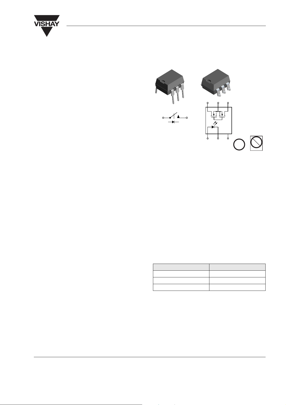
DIP
SMD
1 Form A Solid State Relay
Features
• Isolation Test Voltage 5300 V
• Current-limit Protection Built-in
• High-reliability Monolithic output die
• Low Power Consumption
• Clean, Bounce-free Switching
• High Surge Capability
• Surface Mountable
• Lead-free component
• Component in accordance to RoHS 2002/95/EC
and WEEE 2002/96/EC
Agency Approvals
• UL1577, File No. E52744 System Code H or J,
Double Protection
• CSA - Certification 093751
• BSI/BABT Cert. No. 7980
• DIN EN 60747-5-2 (VDE0884)
DIN EN 60747-5-5 pending
• FIMKO Approval
Applications
General Telecom Switching
- On/off-hook
- Ring Relay/ Dial Pulse
- Ground Start/ Fault Protection
Instrumentation
- Automatic Tuning/Balancing
- Flying Capacitor
- Analog Multiplex
Industrial Controls
- Triac Predrivers
- Output Modules
RMS
LH1510AAB/ AABTR/ AT
Vishay Semiconductors
e3
Peripherals - Transducer Driver
Description
The LH1510 is a SPST normally open switch (1 Form
A) that can replace electromechanical relays in many
applications. The relay is constructed using a GaAlAs
LED for actuation control and an integrated monolithic
die for the switch output. The die, fabricated in a highvoltage dielectrically isolated technology, is comprised of a photodiode array, switch control circuity,
and MOSFET switches. In addition, the relay employs
current-limiting circuity enabling it to pass FCC
68.302 and other regulatory voltage surge requirements when overvoltage protection is provided. The
LH1510 is the only relay in the family that provides
current limiting for unidirectional dc applications.
Order Information
Part Remarks
LH1510AAB Tubes, SMD-6
LH1510AABTR Tape and Reel, SMD-6
LH1510AT Tubes, DIP-6
Pb
Pb-free
Document Number 83810
Rev. 1.3, 26-Oct-04
www.vishay.com
1
Page 2
LH1510AAB/ AABTR/ AT
Vishay Semiconductors
Absolute Maximum Ratings, T
amb
= 25 °C
Stresses in excess of the absolute Maximum Ratings can cause permanent damage to the device. Functional operation of the device is
not implied at these or any other conditions in excess of those given in the operational sections of this document. Exposure to absolute
Maximum Ratings for extended periods of time can adversely affect reliability.
SSR
Parameter Test condition Symbol Val ue Unit
LED continuous forward current I
LED reverse voltage I
DC or peak AC load voltage I
≤ 10 µAV
R
≤ 50 µAV
L
Continuous DC load current bidirectional operation
Continuous DC load current unidirectional operation
Peak load current (single shot) t = 100 ms I
Ambient temperature range T
Storage temperature range T
Pin soldering temperature t = 10 s max T
Input/output isolation voltage V
Output power dissipation
(continuous)
1)
Refer to Current Limit Performance Application Note 58 for a discussion on relay operation during transient currents.
F
R
L
I
L
I
L
P
amb
stg
sld
ISO
P
diss
50 mA
8.0 V
200 V
200 mA
350 mA
1)
- 40 to + 85 °C
- 40 to + 150 °C
260 °C
5300 V
RMS
550 mW
Electrical Characteristics, T
amb
= 25 °C
Minimum and maximum values are testing requirements. Typical values are characteristics of the device and are the result of engineering
evaluations. Typical values are for information only and are not part of the testing requirements.
Input
Parameter Test condition Symbol Min Ty p. Max Unit
LED forward current,
switch turn-on
LED forward current,
switch turn-off
LED forward voltage I
= 100 mA, t = 10 ms I
I
L
= ± 150 V I
V
L
= 10 mA V
F
Fon
Foff
0.2 0.85 mA
F
1.15 1.27 1.45 V
0.95 2.0 mA
Output
Parameter Test condition Symbol Min Ty p. Max Unit
ON-resistance ac/dc:
Pin 4(±) to 6 (±)
ON-resistance dc:
Pin 4, 6 (+) to 5 (±)
Off-resistance I
Current limit ac/dc:
Pin 4 (±) to 6 (±)
Current limit dc:
Pin 4, 6 (+) to 5 (±)
Off-state leakage current I
= 5.0 mA, IL = 50 mA R
I
F
= 5.0 mA, IL = 100 mA R
I
F
= 0 mA, VL = ± 100 V R
F
I
= 5.0 mA, VL = ± 5.0 V,
F
t = 5.0 ms
= 5.0 mA, VL = 4.0 V,
I
F
t = 5.0 ms
= 0 mA, VL = ± 100 V I
F
I
= 0 mA, VL = ± 200 V I
F
I
LMT
I
LMT
ON
ON
OFF
O
O
6.0 11.27 15 Ω
1.5 3.15 3.75 Ω
0.5 80 GΩ
300 368 450 mA
600 736 920 mA
2.36 200 nA
79.2 1.0 µA
www.vishay.com
2
Document Number 83810
Rev. 1.3, 26-Oct-04
Page 3
LH1510AAB/ AABTR/ AT
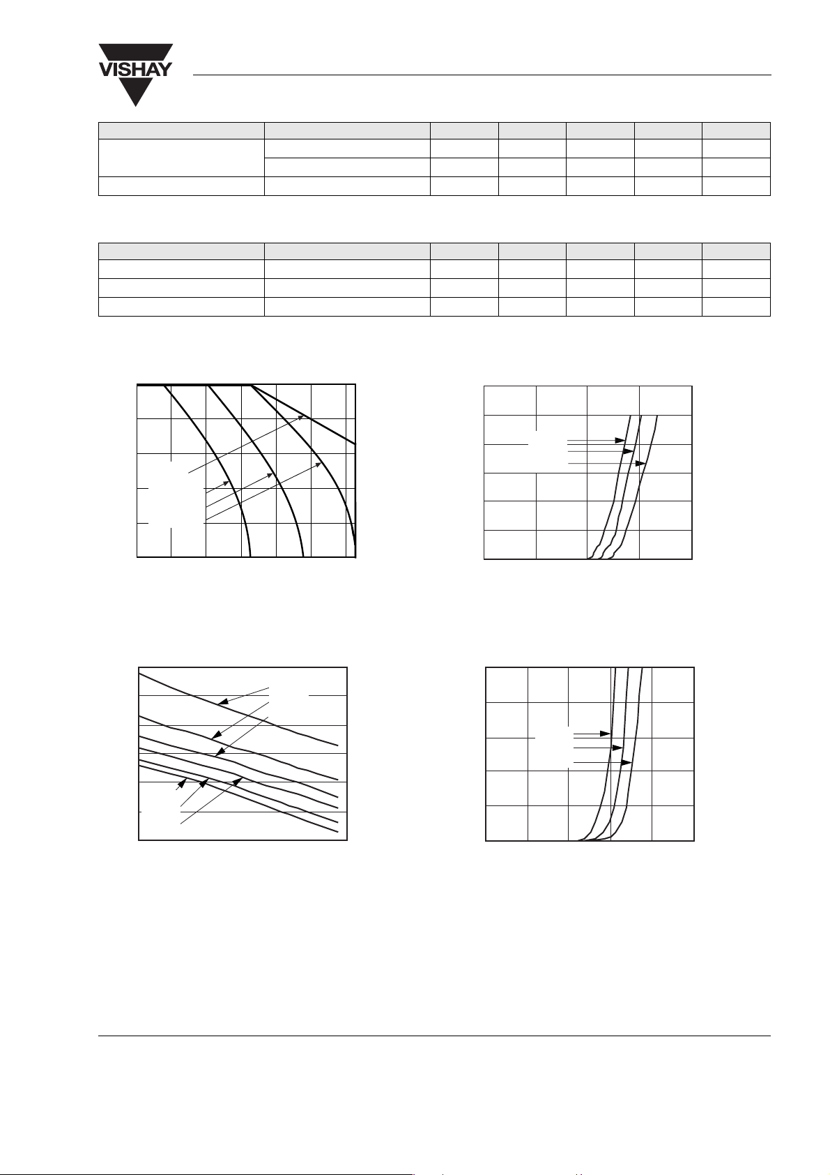
ilh1510at_02
LED Forward Current (mA)
0
20
40
60
80
100
120
0 0.5 1 1.5 2
LED Forward Voltage (V)
T=85°C
T=25°C
T=-40°C
ilh1510at_03
0
2
4
6
8
10
01632486480
LED Reverse Voltage (V)
LED Reverse current (µA)
T=-40°C
T=25°C
T=85°C
Vishay Semiconductors
Parameter Test condition Symbol Min Ty p . Max Unit
Output capacitance Pin 4 to 6 IF = 0 mA, VL = 1.0 V C
I
= 0 mA, VL = 50 V C
F
Switch offset I
= 5.0 mA V
F
O
O
OS
Transfer
Parameter Test condition Symbol Min Ty p . Max Unit
Capacitance (input-output) V
Turn-on time I
Turn-off time I
= 1.0 V C
ISO
= 5.0 mA, IL = 50 mA t
F
= 5.0 mA, IL = 50 mA t
F
IO
on
off
Typical Characteristics (Tamb = 25 °C unless otherwise specified)
200
160
120
I
=
Fon
5.0to20mA
80
I
=2.0 mA
Fon
I
=3.0 mA
Fon
Load Current (mA)
I
Fon
=2.0 mA
40
27.75 pF
10.82 pF
0.17 µV
0.72 pF
0.5 2.0 ms
0.7 2.0 ms
0
-40 -20 0 20 40 60 80
ilh1510at_00
Ambient Temperature (°C)
Figure 1. Recommended Operating Conditions
1.6
1.5
1.4
1.3
1.2
LED Forward Voltage (V)
1.1
1
-40 -20 806040200
ilh1510at_01
IF=1mA
IF=2mA
IF=5mA
Temperature (°C)
IF=50mA
IF=20mA
IF=10mA
Figure 2. LED Voltage vs. Temperature
Figure 3. LED Forward Current vs. LED Forward Voltage
Figure 4. LED Reverse Current vs. LED Reverse Voltage
Document Number 83810
Rev. 1.3, 26-Oct-04
www.vishay.com
3
Page 4

LH1510AAB/ AABTR/ AT
ilh1510at_07
DC Load Currentt (mA)
0
200
400
600
800
1000
01 23 4 5
Load Voltage (V)
T=-40°C
T=25°C
T=85°C
ilh1510at_08
-45
-30
-15
0
15
30
45
-40 -20 0 20 40 60 80
DC Current Limit (%) change,
norm. @25°C
Temperature (°C)
IF=5 mA
T=5ms
VL=4V
ilh1510at_09
-30
-20
-10
0
10
20
30
-40 -20
0
20
40
60 80
Temperature (°C)
Change in Current Limit (%),
norm. to 25°C
IF=5 mA
T=5ms
VL=5V
Vishay Semiconductors
7
6
5
T=85°C
T=25°C
4
T=-40°C
3
Load Voltage (V)
2
1
0
01 23 45
ilh1510at_04
LED Current (mA)
Figure 5. LED Current vs. Load Voltage
80
60
40
20
0
norm. to 25°C
-20
-40
LED Current for Switch Turn-On (%),
-60
-40 -20
ilh1510at_05
020406080
Temperature (°C)
Figure 6. LED Current for Switch Turn-on vs. Temperature
Figure 8. DC Load Current vs. Load Voltage
Figure 9. DC Current Limit vs. Temperature
1.24
1.2
1.16
1.12
LED Dropout Voltage (V)
1.08
1.04
-40 -20 0
ilh1510at_06
20 40 60 80
Temperature (°C)
Figure 7. LED Dropout Voltage vs. Temperature
www.vishay.com
4
IL=100mA
Figure 10. Current Limit vs. Temperature
Document Number 83810
Rev. 1.3, 26-Oct-04
Page 5

500
ilh1510at_13
0
15
30
45
60
75
90
0 20406080100
Capacitance (pF)
Applied Voltage (V)
ilh1510at_14
0
0.02
0.04
0.06
0.08
0.1
0.12
0.14
Insertion Loss (dB)
Frequence (Hz)
10
2
10
3
10
4
10
5
RL=600ıΩ
ilh1510at_15
Leakage Current (nA)
1.0
10.0
100.0
0 40 80 120 160 200
Load Voltage (V)
T=85°C
T=70°C
T=50°C
T=25°C
1000.0
0.1
400
T=-40°C
300
T=25°C
T=85°C
200
Load Current (mA)
100
0
012345
ilh1510at_10
Load Voltage (V)
Figure 11. Load Current vs. Load Voltage
40
30
LH1510AAB/ AABTR/ AT
Vishay Semiconductors
Figure 14. Switch Terminal Capacitance vs. Applied Voltage
20
10
0
norm. to 25°C
-10
Change in On-Resistance (%),
-20
-30
-40 -20 0 20 40 60 80
ilh1510at_11
Temperature (°C)
IF=5mA
IL=50mA
Figure 12. ON-Resistance vs. Temperature
10
8
IL=50mA
6
=5mA
4
F
at I
2
ac/dc R-on Variation (%), norm.
0
-2
0 4 8 12 16 20
ilh1510at_12
LED Current (mA)
Figure 13. Variation in ON-Resistance vs. LED Current
Figure 15. Insertion Loss vs. Frequency
Figure 16. Leakage Current vs. Applied Voltage
Document Number 83810
Rev. 1.3, 26-Oct-04
www.vishay.com
5
Page 6

LH1510AAB/ AABTR/ AT
ilh1510at_19
20 40
Ambient Temperature (°C)
3.5
0
50 706030
3.0
1.5
2.0
2.5
0.5
1.0
80 90
IF= 5.0 mA
Switch Offset Voltage (µV)
ilh1510at_20
010
LED Forward Current (mA)
0.6
0
15 25205
0.5
0.2
0.3
0.4
0.1
Switch Offset Voltage (µV)
ilh1510at_21
Temperature (°C)
Change in Turn-On Time (%),
norm. to 25°C
-16
-24
-8
0
8
16
24
-40 -20 0
20 40 60 80
IF=5mA
IL=50mA
Vishay Semiconductors
120
100
80
60
Isolation (dB)
40
VP=10V
20
RL=50Ωı
0
ilh1510at_16
50
10
3
10
4
10
5
Frequency (Hz)
Figure 17. Output Isolation
10
6
Figure 20. Switch Offset Voltage vs. Temperature
40
30
20
Load Current (µA)
10
0
0 50 100 150 200 250 300
ilh1510at_17
Figure 18. Switch Breakdown Voltage vs. Load Current
9
6
3
0
norm. to 25°C
-3
-6
Change in Breakdown Voltage (%),
-9
-40-20 0 20406080
ilh1510at_18
Figure 19. Switch Breakdown Voltage vs. Temperature
www.vishay.com
6
T=-40°C
T=25°C
T=85°C
IF=0mA
IL<51uA
Load Voltage (V)
Temperature (°C)
Figure 21. Switch Offset Voltage vs. LED Current
IF=0mA
IL<51uA
Figure 22. Turn-on Time vs. Temperature
Document Number 83810
Rev. 1.3, 26-Oct-04
Page 7

norm. to 25°C
Change in Turn-Off Time (%),
ilh1510at_22
30
20
10
0
-10
-40 -20
IF=5mA
IL=50mA
0
40 60 80
20
Temperature (°C)
-20
-30
Figure 23. Turn-off Time vs. Temperature
1.8
LH1510AAB/ AABTR/ AT
Vishay Semiconductors
1.4
T=85°C
1.0
Turn-On Time (ms)
0.6
0.2
01020304050
ilh1510at_23
T=25°C
LED Forward Current (mA)
T=-40°C
IL=50mA
Figure 24. Turn-on Time vs. LED Current
1.0
0.9
0.8
0.7
0.6
Turn-Off Time (ms)
0.5
T=-40°C
T=25°C
T=85°C
IL=50mA
0.4
010203040 50
ilh1510at_24
LED Forward Current (mA)
Figure 25. Turn-off Time vs. LED Current
Document Number 83810
Rev. 1.3, 26-Oct-04
www.vishay.com
7
Page 8
LH1510AAB/ AABTR/ AT
Vishay Semiconductors
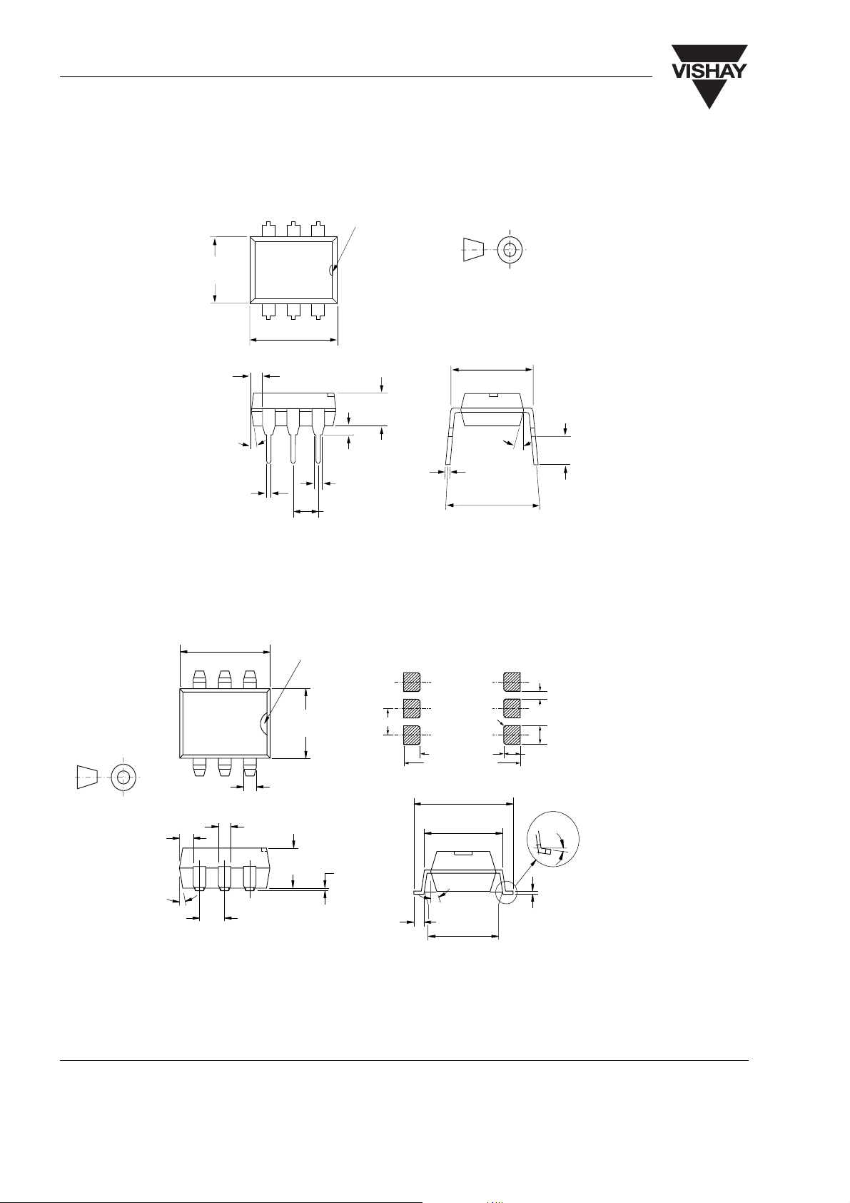
Package Dimensions in Inches (mm)
DIP
Pin One ID.
3
12
.256 (6.50)
.248 (6.30)
4
5
6
.343 (8.70)
.335 (8.50)
.039
(1.00)
Min.
4° Typ.
.020 (.051) Min.
.022 (0.55)
.018 (0.45)
i178001
.035 (0.90)
.031 (0.80)
.100 (2.54) Typ.
Package Dimensions in Inches (mm)
SMD
.343 (8.71)
.335 (8.51)
Pin one I.D.
.150 (3.81)
.130 (3.30)
ISOMethodA
.300 (7.62)
Typ.
18° Typ.
.014 (.35)
.010 (.25)
.347 (8.82)
.300 (7.62)
.150 (3.81)
.110 (2.79)
ISO Method A
i178002
www.vishay.com
8
.039
(0.99)
min.
.030 (.76)
.256 (6.50)
.248 (6.30)
.050 (1.27) typ.
.052 (1.33)
.048 (1.22)
.150 (3.81)
.130 (3.30)
4°
.100 (2.54)
.100 (2.54)
.0098 (.25)
.0040 (.10)
.040 (1.016)
.020 (0.508)
R .010 (.25)
.315 (8.00) min
.435 (11.05)
.395 (10.03)
.375 (9.63)
.300 (7.62)
typ.
18°
.315 (8.00)
min.
.070 (1.78)
.060 (1.52)
3° to 7°
.012 (0.31)
.008 (0.20)
Document Number 83810
Rev. 1.3, 26-Oct-04
Page 9

LH1510AAB/ AABTR/ AT
Vishay Semiconductors
Ozone Depleting Substances Policy Statement
It is the policy of Vishay Semiconductor GmbH to
1. Meet all present and future national and international statutory requirements.
2. Regularly and continuously improve the performance of our products, processes, distribution and
operatingsystems with respect to their impact on the health and safety of our employees and the public, as
well as their impact on the environment.
It is particular concern to control or eliminate releases of those substances into the atmosphere which are
known as ozone depleting substances (ODSs).
The Montreal Protocol (1987) and its London Amendments (1990) intend to severely restrict the use of ODSs
and forbid their use within the next ten years. Various national and international initiatives are pressing for an
earlier ban on these substances.
Vishay Semiconductor GmbH has been able to use its policy of continuous improvements to eliminate the use
of ODSs listed in the following documents.
1. Annex A, B and list of transitional substances of the Montreal Protocol and the London Amendments
respectively
2. Class I and II ozone depleting substances in the Clean Air Act Amendments of 1990 by the Environmental
Protection Agency (EPA) in the USA
3. Council Decision 88/540/EEC and 91/690/EEC Annex A, B and C (transitional substances) respectively.
Vishay Semiconductor GmbH can certify that our semiconductors are not manufactured with ozone depleting
substances and do not contain such substances.
We reserve the right to make changes to improve technical design
and may do so without further notice.
Parameters can vary in different applications. All operating parameters must be validated for each
customer application by the customer. Should the buyer use Vishay Semiconductors products for any
unintended or unauthorized application, the buyer shall indemnify Vishay Semiconductors against all
claims, costs, damages, and expenses, arising out of, directly or indirectly, any claim of personal
damage, injury or death associated with such unintended or unauthorized use.
Vishay Semiconductor GmbH, P.O.B. 3535, D-74025 Heilbronn, Germany
Telephone: 49 (0)7131 67 2831, Fax number: 49 (0)7131 67 2423
Document Number 83810
Rev. 1.3, 26-Oct-04
www.vishay.com
9
Page 10

Legal Disclaimer Notice
Vishay
Notice
Specifications of the products displayed herein are subject to change without notice. Vishay Intertechnology, Inc.,
or anyone on its behalf, assumes no responsibility or liability for any errors or inaccuracies.
Information contained herein is intended to provide a product description only. No license, express or implied, by
estoppel or otherwise, to any intellectual property rights is granted by this document. Except as provided in Vishay's
terms and conditions of sale for such products, Vishay assumes no liability whatsoever, and disclaims any express
or implied warranty, relating to sale and/or use of Vishay products including liability or warranties relating to fitness
for a particular purpose, merchantability, or infringement of any patent, copyright, or other intellectual property right.
The products shown herein are not designed for use in medical, life-saving, or life-sustaining applications.
Customers using or selling these products for use in such applications do so at their own risk and agree to fully
indemnify Vishay for any damages resulting from such improper use or sale.
Document Number: 91000 www.vishay.com
Revision: 08-Apr-05 1
 Loading...