

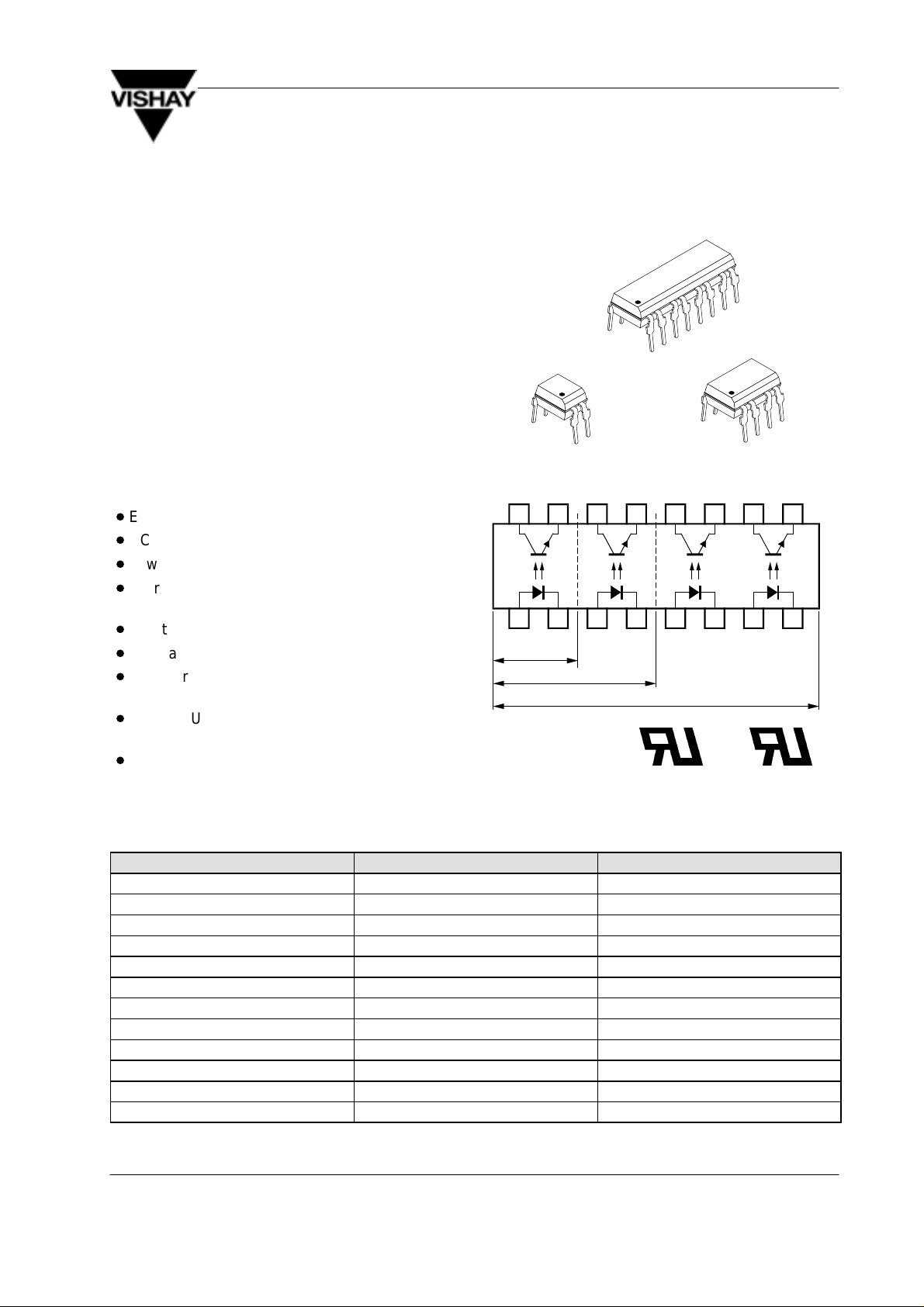
K817P/ K827PH/ K847PH
Optocoupler with Phototransistor Output
Description
The K817P/ K827PH/ K847PH consist of a phototransistor optically coupled to a gallium arsenide
infrared-emitting diode in an 4-lead up to 16-lead
plastic dual inline package.
The elements are mounted on one leadframe using
a coplanar technique, providing a fixed distance
between input and output for highest safety
requirements.
Applications
Programmable logic controllers, modems, answering
machines, general applications
Features
D
Endstackable to 2.54 mm (0.1’) spacing
D
DC isolation test voltage V
D
Low coupling capacitance of typical 0.3 pF
D
Current Transfer Ratio (CTR) selected into
groups
D
Low temperature coefficient of CTR
D
Wide ambient temperature range
D
Underwriters Laboratory (UL) 1577 recognized,
file number E-76222
D
CSA (C–UL) 1577 recognized,
file number E-76222 – Double Protection
D
Coupling System U
= 5 kV
IO
Coll. Emitter
Anode Cath.
4 PIN
8 PIN
16 PIN
C
Vishay Telefunken
14925
13929
Order Instruction
Ordering Code CTR Ranking Remarks
K817P 50 to 600% 4 Pin = Single channel
K827PH 50 to 600% 8 Pin = Dual channel
K847PH 50 to 600% 16 Pin = Quad channel
K817P1 40 to 80% 4 Pin = Single channel
K817P2 63 to 125% 4 Pin = Single channel
K817P3 100 to 200% 4 Pin = Single channel
K817P4 160 to 320% 4 Pin = Single channel
K817P5 50 to 150% 4 Pin = Single channel
K817P6 100 to 300% 4 Pin = Single channel
K817P7 80 to 160% 4 Pin = Single channel
K827P8 130 to 260% 4 Pin = Single channel
K817P9 200 to 400% 4 Pin = Single channel
Rev. A2, 11–Jan–99 177
K817P/ K827PH/ K847PH
Vishay Telefunken
Absolute Maximum Ratings
Input (Emitter)
Parameter Test Conditions Symbol Value Unit
Reverse voltage V
Forward current I
Forward surge current tp ≤ 10 ms I
Power dissipation T
Junction temperature T
Output (Detector)
Parameter Test Conditions Symbol Value Unit
Collector emitter voltage V
Emitter collector voltage V
Collector current I
Peak collector current tp/T = 0.5, tp ≤ 10 ms I
Power dissipation T
Junction temperature T
≤ 25°C P
amb
≤ 25°C P
amb
R
F
FSM
V
CEO
ECO
C
CM
V
6 V
60 mA
1.5 A
100 mW
j
125
°
C
70 V
7 V
50 mA
100 mA
150 mW
j
125
°
C
Coupler
Parameter Test Conditions Symbol V alue Unit
AC isolation test voltage (RMS) t = 1 min VIO
Total power dissipation T
Operating ambient temperature
range
Storage temperature range T
Soldering temperature 2 mm from case, t ≤ 10 s T
1)
Related to standard climate 23/50 DIN 50014
≤ 25°C P
amb
T
tot
amb
stg
sd
1)
5 kV
250 mW
–40 to +100
–55 to +125
260
°
C
°
C
°
C
Rev. A2, 11–Jan–99178
K817P/ K827PH/ K847PH
C F
Vishay Telefunken
Electrical Characteristics (T
amb
= 25°C)
Input (Emitter)
Parameter Test Conditions Symbol Min. Typ. Max. Unit
Forward voltage IF = 50 mA V
Junction capacitance VR = 0 V, f = 1 MHz C
Output (Detector)
Parameter Test Conditions Symbol Min. Typ. Max. Unit
Collector emitter voltage IC = 100 mA V
Emitter collector voltage IE = 100 mA V
Collector dark current VCE = 20 V, IF = 0, E = 0 I
Coupler
Parameter Test Conditions Symbol Min. Typ. Max. Unit
Collector emitter
saturation voltage
Cut-off frequency IF = 10 mA, VCE = 5 V,
Coupling capacitance f = 1 MHz C
IF = 10 mA, IC = 1 mA V
R
L
= 100
W
F
j
CEO
ECO
CEO
CEsat
f
c
k
1.25 1.6 V
50 pF
70 V
7 V
100 nA
0.3 V
100 kHz
0.3 pF
Current Transfer Ratio (CTR)
Parameter Test Conditions Type Symbol Min. Typ. Max. Unit
IC/I
F
VCE = 5 V, IF = 5 mA K817P CTR 0.5 6.0
VCE = 5 V, IF = 5 mA K827PH CTR 0.5 6.0
VCE = 5 V, IF = 5 mA K847PH CTR 0.5 6.0
VCE = 5 V, IF = 10 mA K817P1 CTR 0.4 0.8
VCE = 5 V, IF = 10 mA K817P2 CTR 0.63 1.25
VCE = 5 V, IF = 10 mA K817P3 CTR 1.0 2.0
VCE = 5 V, IF = 10 mA K817P4 CTR 1.6 3.2
VCE = 5 V, IF = 5 mA K817P5 CTR 0.5 1.5
VCE = 5 V, IF = 5 mA K817P6 CTR 1.0 3.0
VCE = 5 V, IF = 5 mA K817P7 CTR 0.8 1.6
VCE = 5 V, IF = 5 mA K817P8 CTR 1.3 2.6
VCE = 5 V, IF = 5 mA K817P9 CTR 2.0 4.0
Rev. A2, 11–Jan–99 179

K817P/ K827PH/ K847PH
S C L
(g)
S F L
(g)
Vishay Telefunken
Switching Characteristics
Parameter Test Conditions Symbol Typ. Unit
Delay time VS = 5 V, IC = 2 mA, RL = 100 W (see figure 1) t
Rise time
Fall time t
Storage time t
Turn-on time t
Turn-off time t
Turn-on time VS = 5 V, IF = 10 mA, RL = 1 kW (see figure 2) t
Turn-off time
d
t
r
f
s
on
off
on
t
off
3.0
3.0
4.7
0.3
6.0
5.0
9.0
18.0
m
s
m
s
m
s
m
s
m
s
m
s
m
s
m
s
+ 5 V
IC= 2 mA ;
Channel I
Channel II
W
0
RG= 50
tp
T
tp= 50 ms
95 10804
= 0.01
I
I
F
F
W
50
W
100
Figure 1. Test circuit, non-saturated operation
0
RG = 50
t
p
+
T
t
= 50 ms
p
95 10843
0.01
I
F
W
50
W
IF = 10 mA
1 k
+ 5 V
I
C
Channel I
Channel II
W
Adjusted through
input amplitude
Oscilloscope
RL= 1 M
CL= 20 pF
Oscilloscope
R
L
C
L
≥ 1 M
≤ 20 pF
W
W
I
F
0
I
C
100%
90%
10%
0
t
r
t
d
t
on
t
p
tion
t
d
t
r
t
(= td + tr) turn-on time
on
pulse duradelay time
rise time
96 11698
t
p
t
t
s
f
t
off
t
s
t
f
t
(= ts + tf) turn-off time
off
t
t
storage time
fall time
Figure 2. Test circuit, saturated operation
Figure 3. Switching times
Rev. A2, 11–Jan–99180

K817P/ K827PH/ K847PH
Vishay Telefunken
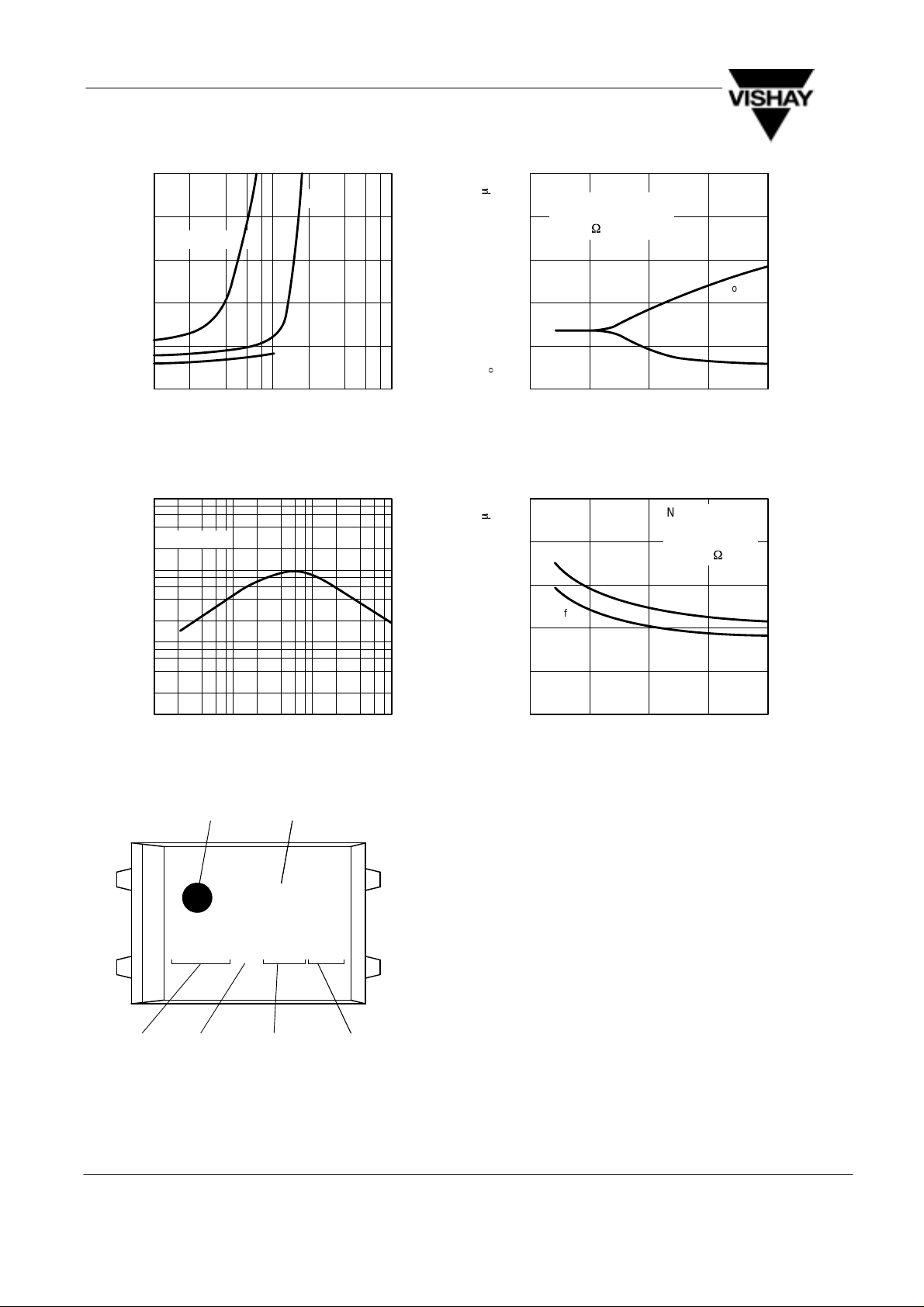
Typical Characteristics (T
300
Coupled device
250
200
Phototransistor
150
IR-diode
100
50
tot
P – Total Power Dissipation ( mW )
0
0 40 80 120
T
96 11700
Figure 4. Total Power Dissipation vs.
1000.0
100.0
– Ambient Temperature (
amb
°
Ambient Temperature
= 25_C, unless otherwise specified)
amb
10000
VCE=20V
I
=0
1000
100
with open Base ( nA )
CEO
I – Collector Dark Current,
95 11026
F
10
1
0255075
T
– Ambient Temperature ( °C )
amb
Figure 7. Collector Dark Current vs.
Ambient Temperature
100
VCE=5V
10
100
10.0
1.0
F
I – Forward Current ( mA )
0.1
0 0.2 0.4 0.6 0.8 1.0 1.2 1.4 1.6 1.8 2.0
VF – Forward Voltage ( V )96 11862
Figure 5. Forward Current vs. Forward Voltage
2.0
VCE=5V
I
=5mA
1.5
1.0
0.5
rel
CTR – Relative Current Transfer Ratio
0
–25 0 25 50
T
– Ambient Temperature ( °C )95 11025
amb
F
75
Figure 6. Relative Current Transfer Ratio vs.
Ambient Temperature
1
0.1
C
I – Collector Current ( mA )
95 11027
0.01
0.1 1 10
IF – Forward Current ( mA )
100
Figure 8. Collector Current vs. Forward Current
100
20mA
IF=50mA
10mA
5mA
2mA
1mA
100
C
I – Collector Current ( mA )
95 10985
10
1
0.1
0.1 1 10
V
– Collector Emitter Voltage ( V )
CE
Figure 9. Collector Current vs. Collector Emitter Voltage
Rev. A2, 11–Jan–99 181
K817P/ K827PH/ K847PH
)
Vishay Telefunken
1.0
20%
0.8
CTR=50%
0.6
0.4
0.2
0
CEsat
V – Collector Emitter Saturation Voltage ( V
110
95 11028
IC – Collector Current ( mA )
10%
100
Figure 10. Collector Emitter Saturation Voltage vs.
Collector Current
1000
VCE=5V
100
10
50
m
off
on
t / t – Turn on / Turn off Time ( s )
95 11031
Saturated Operation
V
=5V
40
30
20
10
S
R
=1k
W
L
0
0 5 10 15
– Forward Current ( mA )
I
F
t
off
t
on
20
Figure 12. Turn on / off Time vs. Forward Current
m
10
8
6
4
t
on
t
off
Non Saturated
Operation
V
=5V
S
R
=100
W
L
2
CTR – Current Transfer Ratio ( % )
95 11029
1
0.1 1 10
IF – Forward Current ( mA )
100
Figure 11. Current Transfer Ratio vs. Forward Current
Pin 1 Indication
Type
off
on
t / t – Turn on / Turn off Time ( s )
95 11030
0
02 4 6
– Collector Current ( mA )
I
C
10
Figure 13. Turn on / off Time vs. Collector Current
K817P
820UTK63
Date
Code
(YM)
Coupling
System
Indicator
Company
Logo
Figure 14. Marking example
15080
Production
Location
Rev. A2, 11–Jan–99182
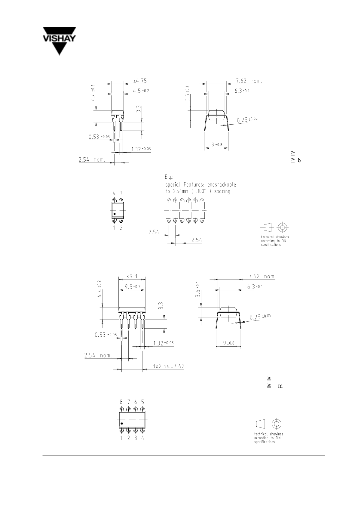
Dimensions of K817P. in mm
K817P/ K827PH/ K847PH
Vishay Telefunken
weight: ca. 0.25 g
creepage distance:y 6 mm
air path:
after mounting on PC board
y
6 mm
Dimensions of K827PH in mm
weight: ca. 0.55 g
creepage distance:
air path:
after mounting on PC board
y
y
6 mm
6 mm
14789
14784
Rev. A2, 11–Jan–99 183

K817P/ K827PH/ K847PH
Vishay Telefunken
Dimensions of K847PH in mm
weight: ca. 1.0 g
creepage distance:y 6 mm
air path:
y
6 mm
after mounting on PC board
14783
Rev. A2, 11–Jan–99184
 Loading...