K814P/ K824P/ K844P
Vishay Semiconductors
Optocoupler, Phototransistor Output, AC input
Features
• Endstackable to 2.54 mm (0.1") spacing
• DC isolation test voltage V
• Low coupling capacitance of typical 0.3 pF
• Current Transfer Ratio (CTR) of typical 100 %
• Low temperature coefficient of CTR
• Wide ambient temperature range
• Lead-free component
• Component in accordance to RoHS 2002/95/EC
and WEEE 2002/96/EC
= 5000 V
ISO
RMS
CE
Agency Approvals
• UL1577, File No. E76222 System Code U, Double
Protection
• C-UL CSA 22.2, Bulletin 5A
Applications
Feature phones, answering machines, PBX, fax
machines
Description
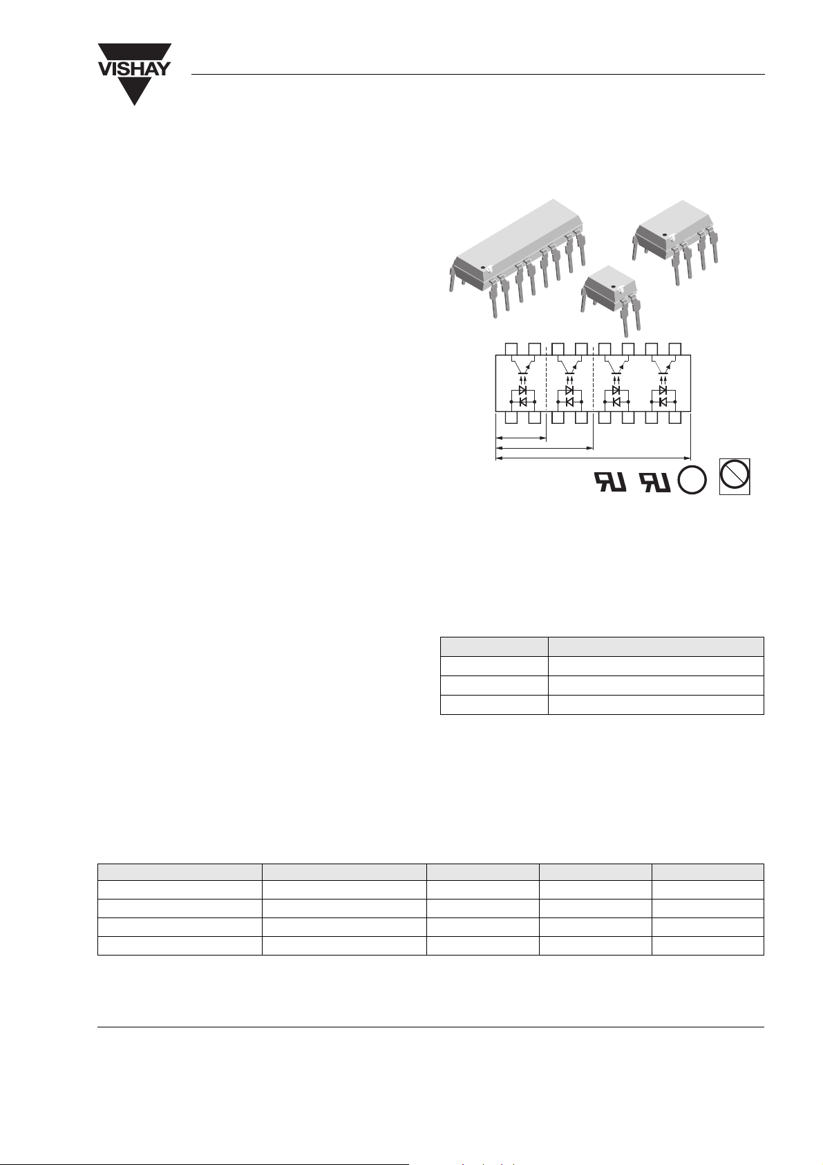
The K814P/ K824P/ K844P consist of a phototransistor optically coupled to 2 gallium arsenide infrared
emitting diodes (reverse polarity) in 4-pin (single); 8
pin (dual) or 16-pin (quad) plastic dual inline package.
17220_1
The elements are mounted on one leadframe providing a fixed distance between input and output for highest safety requirements.
Order Information
K814P CTR > 20 %, Single Channel, DIP-4
K824P CTR > 20 %, Dual Channel, DIP-8
K844P CTR > 20 %, Quad Channel, DIP-16
AC
4PIN
8 PIN
16 PIN
C
Part Remarks
e3
Pb
Pb-free
Absolute Maximum Ratings
T
= 25 °C, unless otherwise specified
amb
Stresses in excess of the absolute Maximum Ratings can cause permanent damage to the device. Functional operation of the device is
not implied at these or any other conditions in excess of those given in the operational sections of this document. Exposure to absolute
Maximum Rating for extended periods of the time can adversely affect reliability.
Input
Parameter Test condition Symbol Val ue Unit
Forward current I
Forward surge current t
Power dissipation P
Junction temperature T
Document Number 83523
Rev. 1.8, 26-Oct-04
≤ 10 µsI
p
F
FSM
diss
± 60 mA
± 1.5 A
100 mW
j
125 °C
www.vishay.com
1

K814P/ K824P/ K844P
Vishay Semiconductors
Output
Paramete r Test condition Symbol Value Unit
Collector emitter voltage V
Emitter collector voltage V
Collector current I
Collector peak current t
Power dissipation P
Junction temperature T
Coupler
Paramete r Test condition Symbol Value Unit
AC Isolation test voltage (RMS) t = 1 min
Total power dissipation P
Operating ambient temperature
range
Storage temperature range T
Soldering temperature 2 mm from case, t ≤ 10 s T
1)
Related to standard climate 23/50 DIN 50014
/T = 0.5, tp ≤ 10 ms I
p
V
ISO
T
CEO
ECO
C
CM
diss
tot
amb
stg
sld
70 V
7V
50 mA
100 mA
150 mW
j
1)
125 °C
5000 V
RMS
250 mW
- 40 to + 100 °C
- 55 to + 125 °C
260 °C
Electrical Characteristics
T
= 25 °C, unless otherwise specified
amb
Minimum and maximum values are testing requirements. Typical values are characteristics of the device and are the result of engineering
evaluation. Typical values are for information only and are not part of the testing requirements.
Input
Paramete r Test condition Symbol Min Ty p. Max Unit
Forward voltage I
Reverse current V
= ± 50 mA V
F
= ± 6 V I
R
F
R
1.25 1.6 V
10 µA
Output
Paramete r Test condition Symbol Min Ty p. Max Unit
Collector emitter voltage I
Emitter collector voltage I
Collector dark current V
= 100 µAV
C
= 100 µAV
E
= 20 V, IF = 0, E = 0 I
CE
CEO
ECO
CEO
70 V
7V
100 nA
Coupler
Paramete r Test condition Symbol Min Ty p. Max Unit
Collector emitter saturation
= ± 10 mA, IC = 1 mA V
I
F
voltage
Cut-off frequency I
= ± 10 mA, VCE = 5 V,
F
= 100 Ω
R
L
Coupling capacitance f = 1 MHz C
CEsat
f
c
k
100 kHz
0.3 pF
0.3 V
Current Transfer Ratio
Paramete r Test condition Par t Symbol Min Ty p. Max Unit
I
C/IF
www.vishay.com
2
VCE = 5 V, IF = ± 5 mA K814P CTR 20 300 %
Document Number 83523
Rev. 1.8, 26-Oct-04

K814P/ K824P/ K844P
Vishay Semiconductors
Switching Characteristics
Para me te r Test condition Symbol Min Ty p. Max Unit
Delay time V
Rise time V
Fall time V
Storage time V
Turn-on time V
Turn-off time V
Turn-on time V
Turn-off time V
= 5 V, IC = 2 mA, RL = 100 Ω
S
= 5 V, IC = 2 mA, RL = 100 Ω
S
= 5 V, IC = 2 mA, RL = 100 Ω
S
= 5 V, IC = 2 mA, RL = 100 Ω
S
= 5 V, IC = 2 mA, RL = 100 Ω
S
= 5 V, IC = 2 mA, RL = 100 Ω
S
= 5 V, IF = 10 mA, RL = 1 kΩ
S
= 5 V, IF = 10 mA, RL = 1 kΩ
S
(see figure 1)
(see figure 1)
(see figure 1)
(see figure 1)
(see figure 1)
(see figure 1)
(see figure 2)
(see figure 2)
t
d
t
r
t
f
t
s
t
on
t
off
t
on
t
off
3.0 µs
3.0 µs
4.7 µs
0.3 µs
6.0 µs
5.0 µs
9.0 µs
18.0 µs
I
I
F
0
F
+ 5 V
IC = 2 mA;
RG = 50 W
t
p
= 0.01
T
tp = 50 Ps
Channel I
Channel II
50 W 100 W
13343
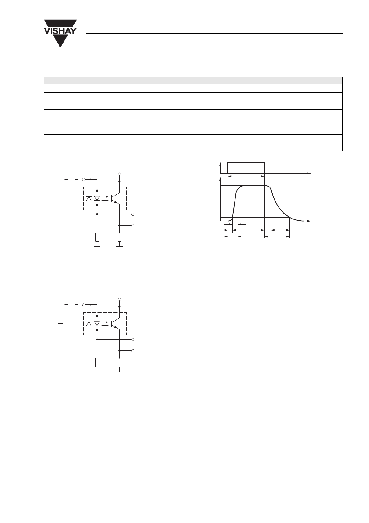
Figure 1. Test circuit, non-saturated operation
0
RG = 50 W
t
p
= 0.01
T
tp = 50 Ps
IF= 10 mA
I
F
50 W 1 kW
+ 5 V
I
C
Channel I
Channel II
adjusted through
input amplitude
Oscilloscope
R
> 1 MW
L
< 20 pF
C
L
Oscilloscope
R
> 1 MW
L
< 20 pF
C
L
I
F
0
I
C
100%
90%
10%
0
t
d
t
t
p
t
d
t
r
t
(= td+tr) turn-on time
on
on
pulse duration
delay time
rise time
t
p
t
r
t
s
t
off
t
s
t
f
t
(= ts+tf) turn-off time
off
Figure 3. Switching Times
96 11698
t
t
f
t
storage time
fall time
13344
Figure 2. Test circuit, saturated operation
Document Number 83523
Rev. 1.8, 26-Oct-04
www.vishay.com
3
 Loading...