

Vishay IRFP450A, SiHFP450A Data Sheet
Power MOSFET
IRFP450A, SiHFP450A
Vishay Siliconix
PRODUCT SUMMARY
VDS (V) 500
R
(Ω)V
DS(on)
Q
(Max.) (nC) 64
g
Q
(nC) 16
gs
Q
(nC) 26
gd
Configuration Single
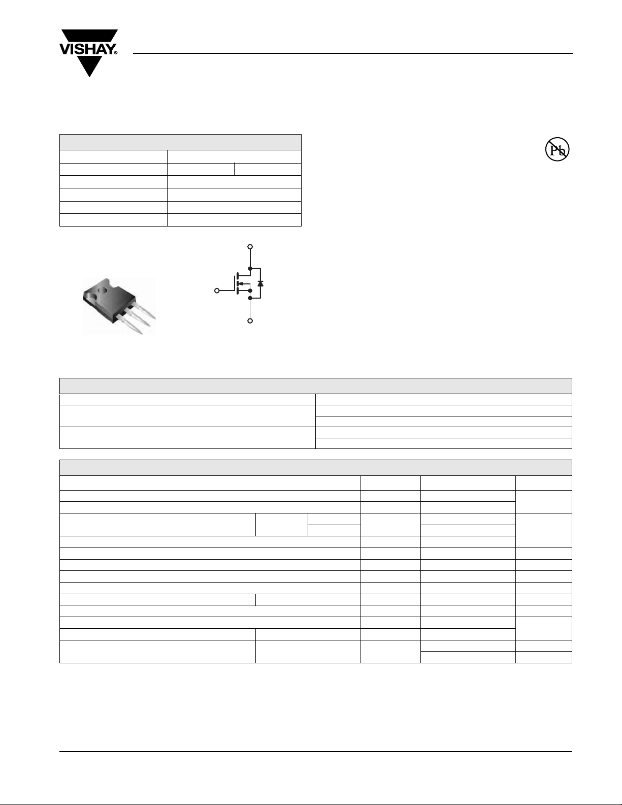
TO-247
= 10 V 0.40
GS
D
FEATURES
• Low Gate Charge Qg Results in Simple Drive
Requirement
• Improved Gate, Avalanche and Dynamic dV/dt
Ruggedness
• Fully Characterized Capacitance and
Avalanche Voltage and Current
• Effective C
• Lead (Pb)-free Available
APPLICATIONS
• Switch Mode Power Supply (SMPS)
G
• Uninterruptable Power Supply
• High Speed Power Switching
S
D
G
N-Channel MOSFET
S
TYPICAL SMPS TOPOLOGIES
• Two Transistor Forward
• Half Bridge, Full Bridge
• PFC Boost
ORDERING INFORMATION
Package TO-247
Lead (Pb)-free
SnPb
IRFP450APbF
SiHFP450A-E3
IRFP450A
SiHFP450A
Specified
oss
Available
RoHS*
COMPLIANT
ABSOLUTE MAXIMUM RATINGS TC = 25 °C, unless otherwise noted
PARAMETER SYMBOL LIMIT UNIT
Drain-Source Voltage V
Gate-Source Voltage V
T
= 25 °C
Continuous Drain Current V
Pulsed Drain Current
a
at 10 V
GS
C
= 100 °C 8.7
C
DS
± 30
GS
I
D
IDM 56
Linear Derating Factor 1.5 W/°C
Single Pulse Avalanche Energy
Repetitive Avalanche Current
Repetitive Avalanche Energy
Maximum Power Dissipation T
Peak Diode Recovery dV/dt
b
a
a
= 25 °C P
c
C
Operating Junction and Storage Temperature Range T
E
AS
I
AR
E
AR
D
dV/dt 4.1 V/ns
, T
J
stg
Soldering Recommendations (Peak Temperature) for 10 s 300
Mounting Torque 6-32 or M3 screw
Notes
a. Repetitive rating; pulse width limited by maximum junction temperature (see fig. 11).
b. Starting T
c. I
SD
= 25 °C, L = 7.8 mH, RG = 25 Ω, IAS = 14 A (see fig. 12).
J
≤ 14 A, dI/dt ≤ 130 A/µs, VDD ≤ VDS, TJ ≤ 150 °C.
d. 1.6 mm from case.
* Pb containing terminations are not RoHS compliant, exemptions may apply
Document Number: 91230 www.vishay.com
S-81271-Rev. A, 16-Jun-08 1
500
14
760 mJ
14 A
19 mJ
190 W
- 55 to + 150
d
10 lbf · in
1.1 N · m
V
AT
°C
IRFP450A, SiHFP450A
Vishay Siliconix
THERMAL RESISTANCE RATINGS
PARAMETER SYMBOL TYP. MAX. UNIT
Maximum Junction-to-Ambient R
Maximum Junction-to-Case (Drain) R
thJA
thCS
thJC
SPECIFICATIONS TJ = 25 °C, unless otherwise noted
PARAMETER SYMBOL TEST CONDITIONS MIN. TYP. MAX. UNIT
Static
Drain-Source Breakdown Voltage V
Temperature Coefficient ΔVDS/TJ Reference to 25 °C, ID = 1 mA - 0.58 -
V
DS
Gate-Source Threshold Voltage V
Gate-Source Leakage I
Zero Gate Voltage Drain Current I
Drain-Source On-State Resistance R
Forward Transconductance g
Dynamic
Input Capacitance C
Output Capacitance C
Reverse Transfer Capacitance C
Output Capacitance C
Output Capacitance C
Effective Output Capacitance C
Total Gate Charge Q
Gate-Drain Charge Q
Turn-On Delay Time t
Rise Time t
Turn-Off Delay Time t
Fall Time t
Drain-Source Body Diode Characteristics
Continuous Source-Drain Diode Current I
Pulsed Diode Forward Current
a
Body Diode Voltage V
Body Diode Reverse Recovery Time t
Body Diode Reverse Recovery Charge Q
Forward Turn-On Time t
Notes
a. Repetitive rating; pulse width limited by maximum junction temperature (see fig. 11).
b. Pulse width ≤ 300 µs; duty cycle ≤ 2 %.
c. C
eff. is a fixed capacitance that gives the same charging time as C
oss
DS
GS(th)
V
GSS
DSS
V
DS(on)
fs
iss
- 307 -
oss
-10-
rss
V
oss
V
oss
eff. VGS = 0 V; VDS = 0 V to 400 V
oss
g
--16
gs
--26
gd
d(on)
r
-35-
d(off)
-29-
f
S
V
V
R
MOSFET symbol
showing the
integral reverse
I
SM
SD
rr
rr
on
p - n junction diode
TJ = 25 °C, IF = 14 A, dI/dt = 100 A/µs
-40
0.24 -
°C/WCase-to-Sink, Flat, Greased Surface R
-0.65
VGS = 0 V, ID = 250 µA 500 - -
VDS = VGS, ID = 250 µA 2.0 - 4.0
= ± 30 V - - ± 100
GS
VDS = 500 V, VGS = 0 V - - 25
= 400 V, VGS = 0 V, TJ = 125 °C - - 250
DS
= 10 V ID = 8.4 A
GS
VDS = 50 V, ID = 8.4 A
VGS = 0 V,
V
= 25 V,
DS
f = 1.0 MHz, see fig. 5
= 0 V; VDS = 1.0 V, f = 1.0 MHz 2859
GS
= 0 V; VDS = 400 V, f = 1.0 MHz 81
GS
b
b
--0.40Ω
7.8 - -
- 2038 -
c
96
--64
= 14 A, VDS = 400 V,
I
= 10 V
GS
D
see fig. 6 and 13
b
-15-
V
= 250 V, ID = 14 A,
DD
= 6.2 Ω, RD = 17 Ω, see fig. 10
G
G
TJ = 25 °C, IS = 14 A, VGS = 0 V
b
D
S
b
-36-
--14
--56
--1.4
- 487 731
b
-3.95.8µC
Intrinsic turn-on time is negligible (turn-on is dominated by LS and LD)
while VDS is rising from 0 to 80 % VDS.
oss
V
V/°C
V
nA
µA
S
pF
nC Gate-Source Charge Q
ns
A
V
ns
www.vishay.com Document Number: 91230
2 S-81271-Rev. A, 16-Jun-08
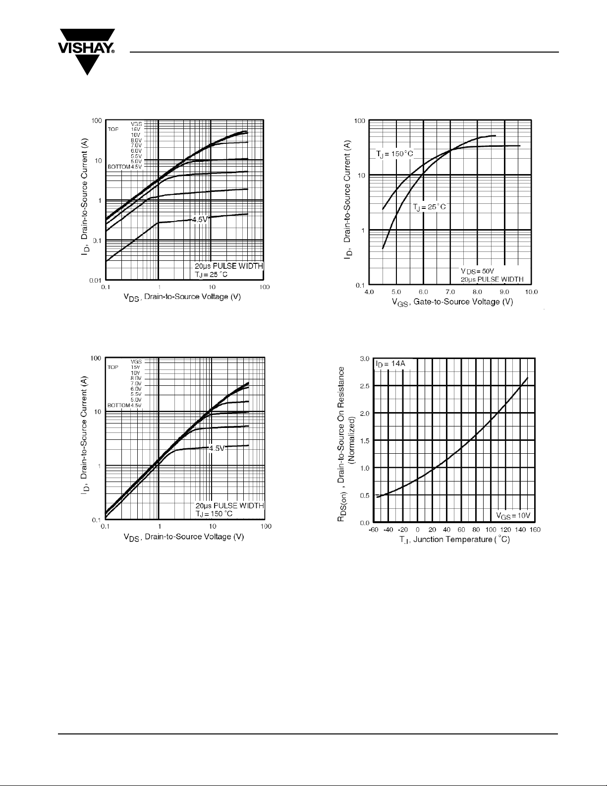
TYPICAL CHARACTERISTICS 25 °C, unless otherwise noted
IRFP450A, SiHFP450A
Vishay Siliconix
Fig. 1 - Typical Output Characteristics
Fig. 2 - Typical Output Characteristics
Fig. 3 - Typical Transfer Characteristics
Fig. 4 - Normalized On-Resistance vs. Temperature
Document Number: 91230 www.vishay.com
S-81271-Rev. A, 16-Jun-08 3
 Loading...