

Vishay IRFP350LC, SiHFP350LC Data Sheet
Power MOSFET
N-Channel MOSFET
G
D
S
TO-247AC
G
D
S
Available
RoHS*
COMPLIANT
IRFP350LC, SiHFP350LC
Vishay Siliconix
PRODUCT SUMMARY
VDS (V) 400
(Ω)V
R
DS(on)
Q
(Max.) (nC) 76
g
Q
(nC) 20
gs
Q
(nC) 37
gd
Configuration Single
= 10 V 0.30
GS
FEATURES
• Ultra Low Gate Charge
• Reduced Gate Drive Requirement
• Enhanced 30V VGS Rating
• Reduced C
• Isolated Central Mounting Hole
• Dynamic dV/dt Rated
• Repetitive Avalanche Rated
• Compliant to RoHS Directive 2002/95/EC
DESCRIPTION
This new series of low charge Power MOSFETs achieve
significantly lower gate charge over conventional MOSFETs.
Utilizing advanced MOSFETs technology the device
improvements allow for reduced gate drive requirements,
faster switching speeds and increased total system savings.
These device improvements combined with the proven
ruggedness and reliability of MOSFETs offer the designer a
new standard in power transistors for switching
applications.
The TO-247AC package is preferred for
commercial-industrial applications where higher power
levels preclude the use of TO-220AB devices. The
TO-247AC is similar but superior to the earlier TO-218
package because of its isolated mounting hole.
ORDERING INFORMATION
Package TO-247AC
Lead (Pb)-free
SnPb
IRFP350LCPbF
SiHFP350LC-E3
IRFP350LC
SiHFP350LC
iss
, C
oss
, C
rss
ABSOLUTE MAXIMUM RATINGS (TC = 25 °C, unless otherwise noted)
PARAMETER SYMBOL LIMIT UNIT
Drain-Source Voltage V
Gate-Source Voltage V
T
= 25 °C
Continuous Drain Current V
Pulsed Drain Current
a
at 10 V
GS
C
= 100 °C 9.9
C
DS
± 30
GS
I
D
IDM 64
Linear Derating Factor 1.5 W/°C
Single Pulse Avalanche Energy
Repetitive Avalanche Current
Repetitive Avalanche Energy
Maximum Power Dissipation T
Peak Diode Recovery dV/dt
b
a
a
= 25 °C P
c
C
Operating Junction and Storage Temperature Range T
E
AS
I
AR
E
AR
D
dV/dt 4.0 V/ns
, T
J
stg
Soldering Recommendations (Peak Temperature) for 10 s 300
Mounting Torque 6-32 or M3 screw
Notes
a. Repetitive rating; pulse width limited by maximum junction temperature (see fig. 11).
= 25 V, starting TJ = 25 °C, L = 2.7 mH, Rg = 25 Ω, IAS = 16 A (see fig. 12).
b. V
DD
≤ 16 A, dI/dt ≤ 200 A/μs, VDD ≤ VDS, TJ ≤ 150 °C.
c. I
SD
d. 1.6 mm from case.
* Pb containing terminations are not RoHS compliant, exemptions may apply
Document Number: 91224 www.vishay.com
S11-0448-Rev. B, 14-Mar-11 1
THE PRODUCT DESCRIBED HEREIN AND THIS DATASHEET ARE SUBJECT TO SPECIFIC DISCLAIMERS, SET FORTH AT
This datasheet is subject to change without notice.
400
16
390 mJ
16 A
19 mJ
190 W
- 55 to + 150
d
10 lbf · in
1.1 N · m
www.vishay.com/doc?91000
V
AT
°C
IRFP350LC, SiHFP350LC
S
D
G
Vishay Siliconix
THERMAL RESISTANCE RATINGS
PARAMETER SYMBOL TYP. MAX. UNIT
Maximum Junction-to-Ambient R
Maximum Junction-to-Case (Drain) R
thJA
thCS
thJC
SPECIFICATIONS (TJ = 25 °C, unless otherwise noted)
PARAMETER SYMBOL TEST CONDITIONS MIN. TYP. MAX. UNIT
Static
Drain-Source Breakdown Voltage V
Temperature Coefficient ΔVDS/TJ Reference to 25 °C, ID = 1 mA - 0.49 -
V
DS
Gate-Source Threshold Voltage V
Gate-Source Leakage I
Zero Gate Voltage Drain Current I
Drain-Source On-State Resistance R
Forward Transconductance g
Dynamic
Input Capacitance C
Reverse Transfer Capacitance C
Total Gate Charge Q
Gate-Drain Charge Q
Turn-On Delay Time t
Rise Time t
Turn-Off Delay Time t
Fall Time t
Drain-Source Body Diode Characteristics
Continuous Source-Drain Diode Current I
Pulsed Diode Forward Current
a
Body Diode Voltage V
Body Diode Reverse Recovery Time t
Body Diode Reverse Recovery Charge Q
Forward Turn-On Time t
Notes
a. Repetitive rating; pulse width limited by maximum junction temperature (see fig. 11).
b. Pulse width ≤ 300 μs; duty cycle ≤ 2 %.
DS
GS(th)
V
GSS
DSS
V
DS(on)
fs
iss
- 390 -
oss
-31-
rss
g
--20
gs
--37
gd
d(on)
r
-33-
d(off)
-35-
f
S
I
SM
SD
rr
rr
on
V
V
MOSFET symbol
showing the
integral reverse
p - n junction diode
TJ = 25 °C, IF = 16 A, dI/dt = 100 A/μs
-40
0.24 -
°C/WCase-to-Sink, Flat, Greased Surface R
-0.65
VGS = 0 V, ID = 250 μA 400 - -
VDS = VGS, ID = 250 μA 2.0 -
= ± 20 V - -
GS
VDS = 400 V, VGS = 0 V - -
= 320 V, VGS = 0 V, TJ = 125 °C - -
DS
= 10 V ID = 9.6 A
GS
VDS = 50 V, ID = 9.6 A
VGS = 0 V,
= 25 V,
V
DS
b
b
--
8.1 - -
- 2200 -
4.0 V
± 100 nA
25
250
0.30 Ω
f = 1.0 MHz, see fig. 5
--76
= 16 A, VDS = 320 V
I
= 10 V
GS
D
see fig. 6 and 13
b
-14-
V
= 200 V, ID = 16 A,
DD
R
= 6.2 Ω, RD = 12 Ω, see fig. 10
g
b
-54-
--16
--64
TJ = 25 °C, IS = 16 A, VGS = 0 V
b
--
-
b
-
1.6 V
440 660 ns
4.1 6.2 μC
Intrinsic turn-on time is negligible (turn-on is dominated by LS and LD)
V
V/°C
μA
S
pFOutput Capacitance C
nC Gate-Source Charge Q
ns
A
www.vishay.com Document Number: 91224
2 S11-0448-Rev. B, 14-Mar-11
THE PRODUCT DESCRIBED HEREIN AND THIS DATASHEET ARE SUBJECT TO SPECIFIC DISCLAIMERS, SET FORTH AT
This datasheet is subject to change without notice.
www.vishay.com/doc?91000
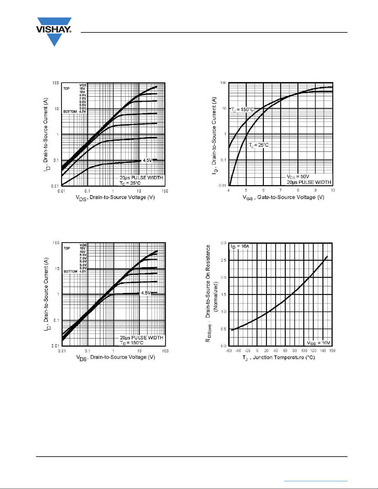
TYPICAL CHARACTERISTICS (25 °C, unless otherwise noted)
IRFP350LC, SiHFP350LC
Vishay Siliconix
Fig. 1 - Typical Output Characteristics, TC = 25 °C
Fig. 2 - Typical Output Characteristics, T
= 150 °C
C
Fig. 3 - Typical Transfer Characteristics
Fig. 4 - Normalized On-Resistance vs. Temperature
Document Number: 91224 www.vishay.com
S11-0448-Rev. B, 14-Mar-11 3
THE PRODUCT DESCRIBED HEREIN AND THIS DATASHEET ARE SUBJECT TO SPECIFIC DISCLAIMERS, SET FORTH AT
This datasheet is subject to change without notice.
www.vishay.com/doc?91000
 Loading...