

Vishay IRFP17N50L, SiHFP17N50L Data Sheet
IRFP17N50L, SiHFP17N50L
N-Channel MOSFET
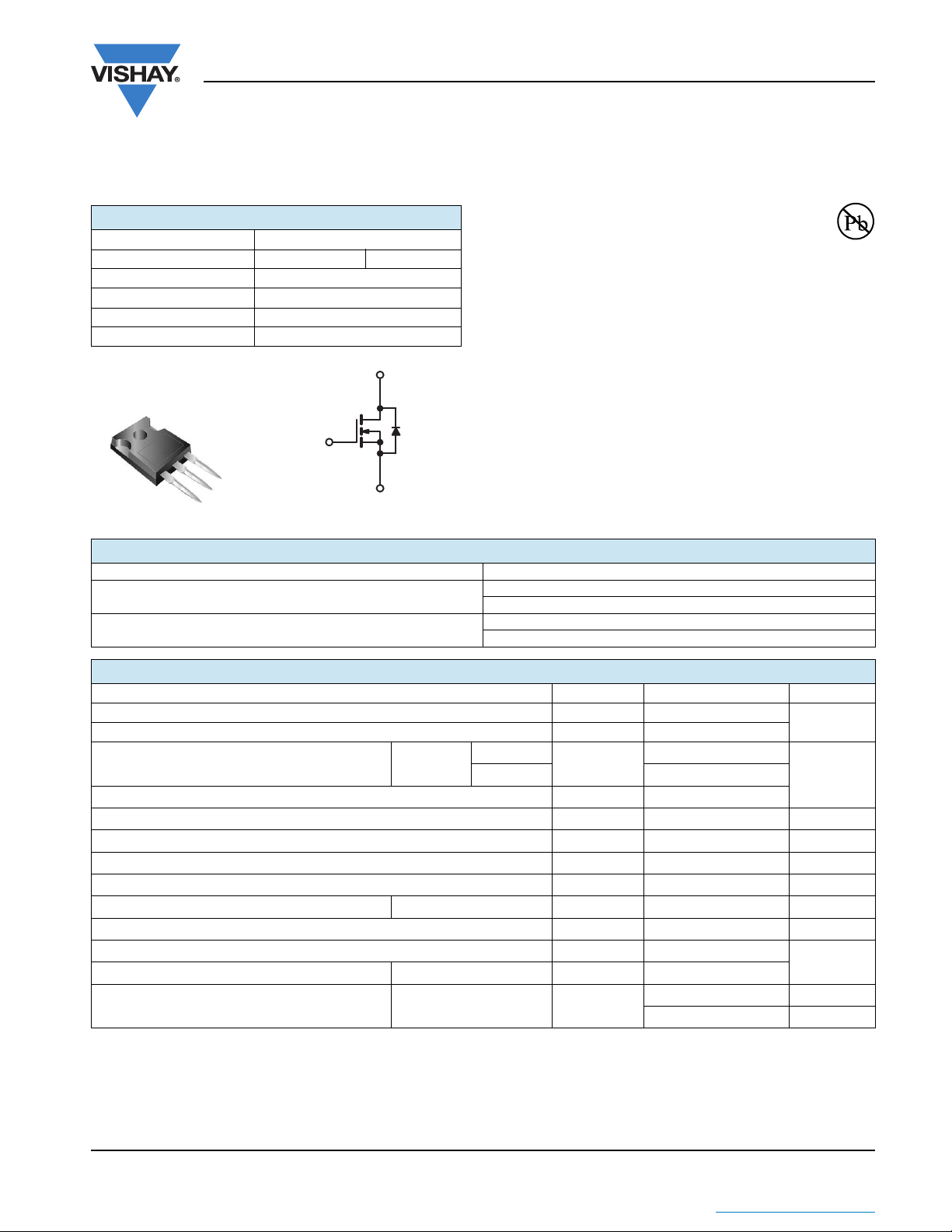
G
D
S
TO-247AC
G
D
S
Available
RoHS*
COMPLIANT
Power MOSFET
Vishay Siliconix
PRODUCT SUMMARY
VDS (V) 500
R
(Ω)V
DS(on)
Q
(Max.) (nC) 130
g
Q
(nC) 33
gs
Q
(nC) 59
gd
Configuration Single
= 10 V 0.28
GS
FEATURES
• SuperFast Body Diode Eliminates the Need
For External Diodes in ZVS Applications
• Low Gate Charge Results in Simple Drive
Requirement
• Enhanced dV/dt Capabilities Offer Improved
Ruggedness
• Higher Gate Voltage Threshold Offers Improved Noise
Immunity
• Compliant to RoHS Directive 2002/95/EC
APPLICATIONS
• Zero Voltage Switching SMPS
• Telecom and Server Power Supplies
• Uninterruptible Power Supply
• Motor Control applications
ORDERING INFORMATION
Package TO-247AC
Lead (Pb)-free
SnPb
IRFP17N50LPbF
SiHFP17N50L-E3
IRFP17N50L
SiHFP17N50L
ABSOLUTE MAXIMUM RATINGS (TC = 25 °C, unless otherwise noted)
PARAMETER SYMBOL LIMIT UNIT
Drain-Source Voltage V
Gate-Source Voltage V
= 25 °C
T
Continuous Drain Current V
Pulsed Drain Current
a
at 10 V
GS
C
= 100 °C 11
C
DS
± 30
GS
I
D
IDM 64
Linear Derating Factor 1.8 W/°C
Single Pulse Avalanche Energy
Repetitive Avalanche Current
Repetitive Avalanche Energy
Maximum Power Dissipation T
Peak Diode Recovery dV/dt
Operating Junction and Storage Temperature Range T
b
a
a
= 25 °C P
C
c
E
AS
I
AR
E
AR
D
dV/dt 13 V/ns
, T
J
stg
Soldering Recommendations (Peak Temperature) for 10 s 300
Mounting Torque 6-32 or M3 screw
Notes
a. Repetitive rating; pulse width limited by maximum junction temperature (see fig. 11).
b. Starting T
c. I
SD
d. 1.6 mm from case.
= 25 °C, L = 3.0 mH, Rg = 25 Ω, IAS = 16 A (see fig. 12).
J
≤ 16 A, dI/dt ≤ 347 A/μs, VDD ≤ VDS, TJ ≤ 150 °C.
500
16
390 mJ
16 A
22 mJ
220 W
- 55 to + 150
d
10 lbf · in
1.1 N · m
V
AT
°C
* Pb containing terminations are not RoHS compliant, exemptions may apply
Document Number: 91205 www.vishay.com
S11-0446-Rev. B, 14-Mar-11 1
THE PRODUCT DESCRIBED HEREIN AND THIS DATASHEET ARE SUBJECT TO SPECIFIC DISCLAIMERS, SET FORTH AT
This datasheet is subject to change without notice.
www.vishay.com/doc?91000
IRFP17N50L, SiHFP17N50L
Vishay Siliconix
THERMAL RESISTANCE RATINGS
PARAMETER SYMBOL TYP. MAX. UNIT
Maximum Junction-to-Ambient R
Maximum Junction-to-Case (Drain) R
thJA
thCS
thJC
SPECIFICATIONS (TJ = 25 °C, unless otherwise noted)
PARAMETER SYMBOL TEST CONDITIONS MIN. TYP. MAX. UNIT
Static
Drain-Source Breakdown Voltage V
Temperature Coefficient ΔVDS/TJ Reference to 25 °C, ID = 1 mA
V
DS
Gate-Source Threshold Voltage V
Gate-Source Leakage I
Zero Gate Voltage Drain Current I
Drain-Source On-State Resistance R
Forward Transconductance g
Dynamic
Input Capacitance C
Output Capacitance C
Reverse Transfer Capacitance C
Output Capacitance C
Effective Output Capacitance C
Effective Output Capacitance
(Energy Related)
Internal Gate Resistance R
Total Gate Charge Q
Gate-Drain Charge Q
Turn-On Delay Time t
Rise Time t
Turn-Off Delay Time t
Fall Time t
Drain-Source Body Diode Characteristics
Continuous Source-Drain Diode Current I
Pulsed Diode Forward Current
a
Body Diode Voltage V
Body Diode Reverse Recovery Time t
Body Diode Reverse Recovery Charge Q
Reverse Recovery Current I
Forward Turn-On Time t
Notes
a. Repetitive rating; pulse width limited by maximum junction temperature (see fig. 11).
b. Pulse width ≤ 300 μs; duty cycle ≤ 2 %.
eff. is a fixed capacitance that gives the same charging time as C
c. C
OSS
eff. (ER) is a fixed capacitance that stores the same energy as C
C
OSS
DS
GS(th)
V
GSS
DSS
VGS = 10 V ID = 9.9 A
DS(on)
fs
iss
- 325 -
oss
-37-
rss
oss
eff.
oss
eff. (ER) - 120 -
C
oss
g
g
--33
gs
--59
gd
d(on)
r
-50-
d(off)
-28-
f
S
I
SM
SD
rr
rr
RRM
on
V
V
GS
V
GS
MOSFET symbol
showing the
integral reverse
p - n junction diode
TJ = 25 °C
= 125 °C - 220 330
T
J
TJ = 25 °C - 470 710
= 125 °C - 810 1210
T
J
-62
0.50 -
°C/WCase-to-Sink, Flat, Greased Surface R
-0.56
VGS = 0 V, ID = 250 μA 500 - - V
d
-0.60-V/°C
VDS = VGS, ID = 250 μA 3.0 - 5.0 V
= ± 30 V - - ± 100 nA
GS
VDS = 500 V, VGS = 0 V - - 50 μA
= 400 V, VGS = 0 V, TJ = 125 °C - - 2.0 mA
DS
VDS = 50 V, ID = 9.9 A
VGS = 0 V,
V
DS
= 25 V,
b
b
- 0.28 0.32 Ω
11 - - S
- 2760 -
f = 1.0 MHz, see fig. 5
V
= 1.0 V , f = 1.0 MHz - 3690 -
DS
= 400 V , f = 1.0 MHz - 84 -
V
= 0 V
DS
V
= 0 V to 400 V
DS
- 159 -
f = 1 MHz, open drain - 1.4 - Ω
= 16 A, VDS = 400 V
I
= 10 V
V
R
see fig. 14a and 14b
D
see fig. 7 and 15
= 250 V, ID = 16 A
DD
= 7.5 Ω, V
G
GS
= 10 V
b
G
TJ = 25 °C, IS = 16 A, VGS = 0 V
b
D
S
b
- - 130
-21-
-51-
--16
--64
--1.5V
- 170 250
= 16 A,
I
F
dI/dt = 100 A/μs
b
TJ = 25 °C - 7.3 11
Intrinsic turn-on time is negligible (turn-on is dominated by LS and LD)
while VDS is rising fom 0 % to 80 % VDS.
OSS
while VDS is rising fom 0 % to 80 % VDS.
OSS
pF
nC Gate-Source Charge Q
ns
A
ns
μC
www.vishay.com Document Number: 91205
2 S11-0446-Rev. B, 14-Mar-11
This datasheet is subject to change without notice.
THE PRODUCT DESCRIBED HEREIN AND THIS DATASHEET ARE SUBJECT TO SPECIFIC DISCLAIMERS, SET FORTH AT
www.vishay.com/doc?91000
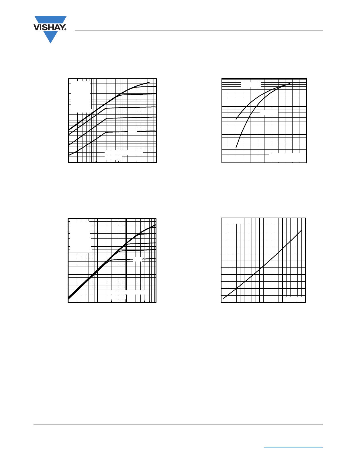
TYPICAL CHARACTERISTICS (25 °C, unless otherwise noted)
0.1 1 10 100
VDS, Drain-to-Source Voltage (V)
0.01
0.1
1
10
100
I
D
,
D
r
a
i
n
-
t
o
-
S
o
u
r
c
e
C
u
r
r
e
n
t
(
A
)
5.0V
20µs PULSE WIDTH
Tj = 25°C
VGS
TOP 15V
12V
10V
8.0V
7.0V
6.0V
5.5V
BOTTOM 5.0V
0.1 1 10 100
VDS, Drain-to-Source Voltage (V)
0.1
1
10
100
I
D
,
D
r
a
i
n
-
t
o
-
S
o
u
r
c
e
C
u
r
r
e
n
t
(
A
)
5.0V
20µs PULSE WIDTH
Tj = 150°C
VGS
TOP 15V
12V
10V
8.0V
7.0V
6.0V
5.5V
BOTTOM 5.0V
0.1
1
10
100
4.0 5.0 6.0 7.0 8.0 9.0 10.0
V = 50V
20µs PULSE WIDTH
DS
V , Gate-to-Source Voltage (V)
I , Drain-to-Source Current (A)
GS
D
T = 150 C
J
°
T = 25 C
J
°
-60 -40 -20 0 20 40 60 80 100 120 140 160
0.0
0.5
1.0
1.5
2.0
2.5
3.0
T , Junction Temperature ( C)
R , Drain-to-Source On Resistance
(Normalized)
J
DS(on)
°
V =
I =
GS
D
10V
16A
IRFP17N50L, SiHFP17N50L
Vishay Siliconix
Fig. 1 - Typical Output Characteristics
Fig. 2 - Typical Output Characteristics
Document Number: 91205 www.vishay.com
S11-0446-Rev. B, 14-Mar-11 3
THE PRODUCT DESCRIBED HEREIN AND THIS DATASHEET ARE SUBJECT TO SPECIFIC DISCLAIMERS, SET FORTH AT
Fig. 3 - Typical Transfer Characteristics
Fig. 4 - Normalized On-Resistance vs. Temperature
This datasheet is subject to change without notice.
www.vishay.com/doc?91000
 Loading...