

Vishay IRFIBC40GLC, SiHFIBC40GLC Data Sheet
www.vishay.com
N-Channel MOSFET
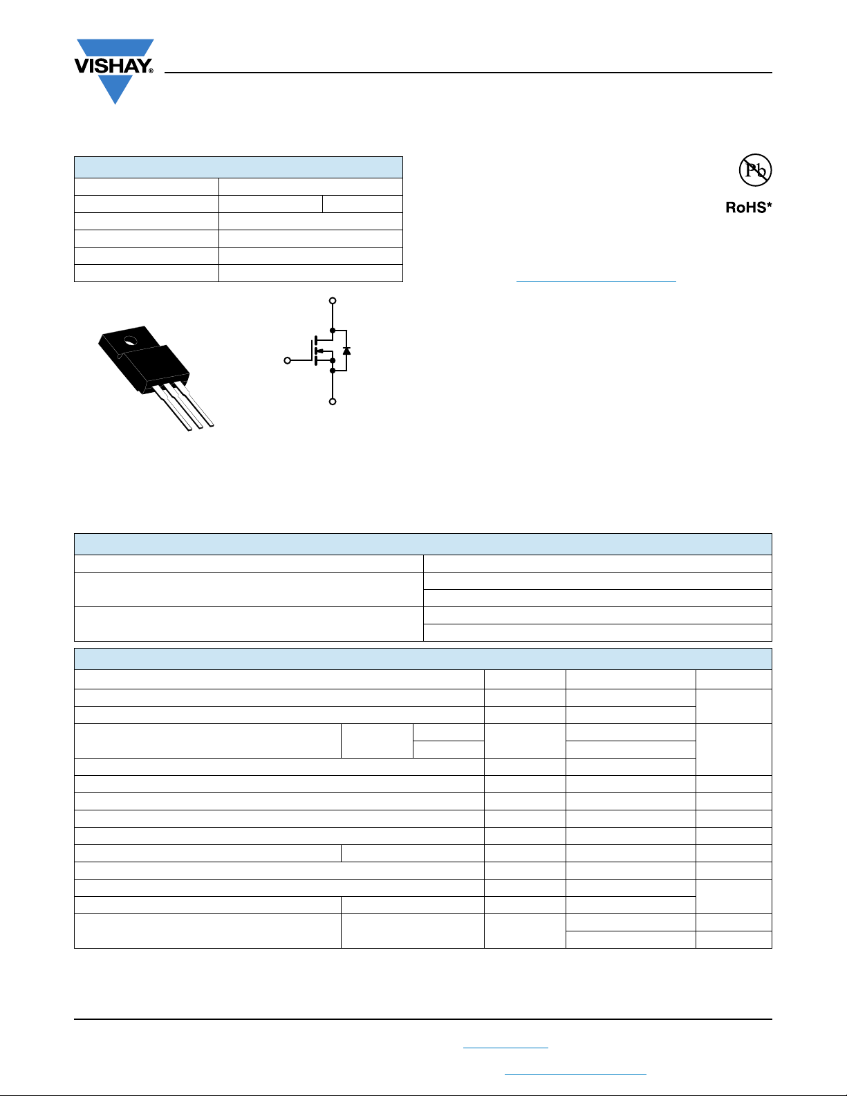
G
D
S
S
D
G
TO-220 FULLPAK
IRFIBC40GLC, SiHFIBC40GLC
Vishay Siliconix
Power MOSFET
PRODUCT SUMMARY
VDS (V) 600
R
()V
DS(on)
Q
max. (nC) 39
g
Q
(nC) 10
gs
Q
(nC) 19
gd
Configuration Single
= 10 V 1.2
GS
FEATURES
• Isolated package
• High voltage isolation = 2.5 kV
f = 60 Hz)
• Sink to lead creepage distance = 4.8 mm
• Dynamic dV/dt rating
• Low thermal resistance
• Material categorization: for definitions of compliance
please see www.vishay.com/doc?99912
Note
*
Thi s datasheet pro vi des information about parts that are
RoHS-compliant and / or parts that are non-RoHS-compliant. For
example, parts with lead (Pb) terminations are not RoHS-compliant.
Please see the information / tables in this datasheet for details.
DESCRIPTION
Third generation power MOSFETs from Vishay provide the
designer with the best combination of fast switching,
ruggedized device design, low on-resistance and
cost-effectiveness.
The TO-220 FULLPAK eliminates the need for additional
insulating hardware in commercial-industrial applications.
The molding compound used provides a high isolation
capability and a low thermal resistance between the tab and
external heatsink. This isolation is equivalent to using a 100
micron mica barrier with standard TO-220 product. The
FULLPAK is mounted to a heatsink using a single clip or by
a single screw fixing.
ORDERING INFORMATION
Package TO-220 FULLPAK
Lead (Pb)-free
SnPb
IRFIBC40GLCPbF
SiHFIBC40GLC-E3
IRFIBC40GLC
SiHFIBC40GLC
(t = 60 s;
RMS
Available
Available
Notes
a. Repetitive rating; pulse width limited by maximum junction temperature (see fig. 11).
b. V
c. ISD 6.2 A, dI/dt 80 A/μs, VDD VDS, TJ 150 °C.
d. 1.6 mm from case.
S16-0763-Rev. B, 02-May-16
ABSOLUTE MAXIMUM RATINGS (TC = 25 °C, unless otherwise noted)
PARAMETER SYMBOL LIMIT UNIT
Drain-Source Voltage V
Gate-Source Voltage V
T
= 25 °C
Continuous Drain Current V
Pulsed Drain Current
a
at 10 V
GS
C
= 100 °C 2.2
C
DS
± 20
GS
I
D
IDM 14
Linear Derating Factor 0.32 W/°C
Single Pulse Avalanche Energy
Repetitive Avalanche Current
Repetitive Avalanche Energy
Maximum Power Dissipation T
Peak Diode Recovery dV/dt
Operating Junction and Storage Temperature Range T
Soldering Recommendations (Peak temperature)
b
a
a
= 25 °C P
c
d
C
for 10 s 300
E
AS
I
AR
E
AR
D
dV/dt 3.0 V/ns
, T
J
stg
Mounting Torque 6-32 or M3 screw
= 50 V, starting TJ = 25 °C, L = 12 μH, RG = 25 , IAS = 3.5 A (see fig. 12).
DD
1
For technical questions, contact: hvm@vishay.com
THIS DOCUMENT IS SUBJECT TO CHANGE WITHOUT NOTICE. THE PRODUCTS DESCRIBED HEREIN AND THIS DOCUMENT
ARE SUBJECT TO SPECIFIC DISCLAIMERS, SET FORTH AT www.vishay.com/doc?91000
600
3.5
320 mJ
3.5 A
4.0 mJ
40 W
-55 to +150
10 lbf · in
1.1 N · m
Document Number: 91181
V
AT
°C
IRFIBC40GLC, SiHFIBC40GLC
D
S
G
S
D
G
www.vishay.com
THERMAL RESISTANCE RATINGS
PARAMETER SYMBOL TYP. MAX. UNIT
Maximum Junction-to-Ambient R
Maximum Junction-to-Case (Drain) R
thJA
thJC
-65
-3.1
SPECIFICATIONS (TJ = 25 °C, unless otherwise noted)
PARAMETER SYMBOL TEST CONDITIONS MIN. TYP. MAX. UNIT
Static
Drain-Source Breakdown Voltage V
V
Temperature Coefficient VDS/TJ Reference to 25 °C, ID = 1 mA - 0.70 - V/°C
DS
Gate-Source Threshold Voltage V
Gate-Source Leakage I
Zero Gate Voltage Drain Current I
Drain-Source On-State Resistance R
Forward Transconductance g
DS
GS(th)
V
GSS
DSS
VGS = 10 V ID = 2.1 A
DS(on)
fs
Dynamic
Input Capacitance C
Output Capacitance C
Reverse Transfer Capacitance C
iss
- 140 -
oss
-15-
rss
Drain to Sink Capacitance C f = 1.0 MHz - 12 -
Total Gate Charge Q
Gate-Drain Charge Q
Turn-On Delay Time t
Rise Time t
Turn-Off Delay Time t
Fall Time t
Internal Drain Inductance L
g
--10
gs
--19
gd
d(on)
r
-27-
d(off)
-17-
f
D
package and center of
Internal Source Inductance L
S
VGS = 0 V, ID = 250 μA 600 - - V
VDS = VGS, ID = 250 μA 2.0 - 4.0 V
= ± 20 V - - ± 100 nA
GS
VDS = 600 V, VGS = 0 V - - 25
= 480 VGS = 0 V, TJ = 125 °C - - 250
V
DS
VDS = 100 V, ID = 3.7 A
b
b
VGS = 0 V,
V
= 25 V,
DS
f = 1.0 MHz, see fig. 5
= 6.2 A, VDS = 360 V,
I
V
GS
= 10 V
V
D
see fig. 6 and 13
= 300 V, ID = 6.2 A,
DD
R
= 9.1 , RD= 47 ,
G
see fig. 10
b
b
Between lead,
6 mm (0.25") from
die contact
Vishay Siliconix
°C/W
μA
--1.2
3.7 - - S
- 1100 -
pF
--39
nC Gate-Source Charge Q
-12-
-20-
-4.5-
-7.5-
ns
nH
Gate Input Resistance R
g
f = 1 MHz, open drain 0.6 - 3.9
Drain-Source Body Diode Characteristics
Continuous Source-Drain Diode Current I
Pulsed Diode Forward Current
a
Body Diode Voltage V
Body Diode Reverse Recovery Time t
Body Diode Reverse Recovery Charge Q
Forward Turn-On Time t
S
I
SM
SD
rr
rr
on
MOSFET symbol
showing the
integral reverse
p - n junction diode
TJ = 25 °C, IS = 3.5 A, VGS = 0 V
b
TJ = 25 °C, IF = 6.2 A, dI/dt = 100 A/μs
Intrinsic turn-on time is negligible (turn-on is dominated by LS and LD)
--3.5
--14
--1.5V
- 440 660 ns
b
-2.13.2μC
A
Notes
a. Repetitive rating; pulse width limited by maximum junction temperature (see fig. 11).
b. Pulse width 300 μs; duty cycle 2 %.
THIS DOCUMENT IS SUBJECT TO CHANGE WITHOUT NOTICE. THE PRODUCTS DESCRIBED HEREIN AND THIS DOCUMENT
ARE SUBJECT TO SPECIFIC DISCLAIMERS, SET FORTH AT www.vishay.com/doc?91000
For technical questions, contact: hvm@vishay.com
S16-0763-Rev. B, 02-May-16
2
Document Number: 91181
IRFIBC40GLC, SiHFIBC40GLC
www.vishay.com
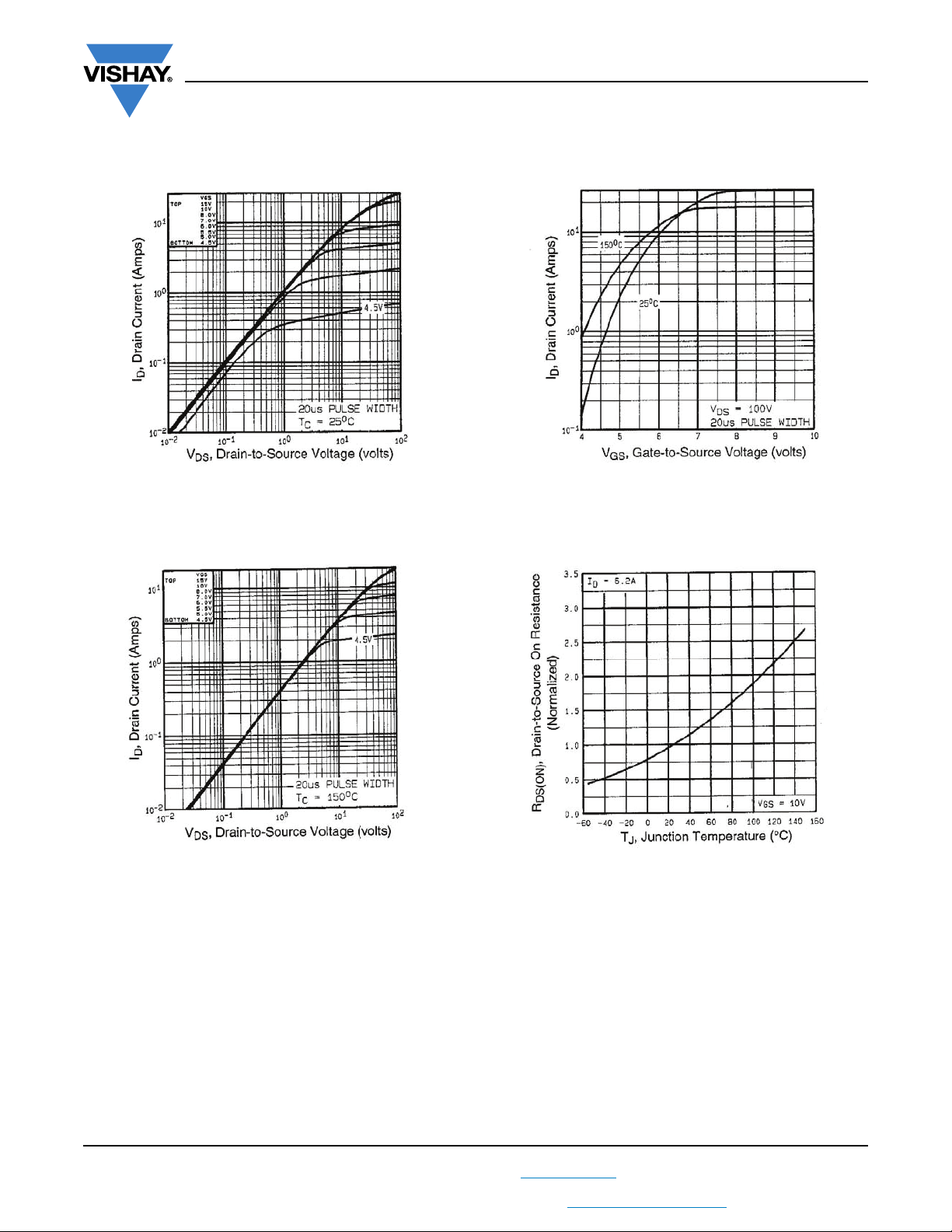
TYPICAL CHARACTERISTICS (25 °C, unless otherwise noted)
Vishay Siliconix
Fig. 1 - Typical Output Characteristics, TC= 25 °C
Fig. 2 - Typical Output Characteristics, T
= 150 °C
C
Fig. 3 - Typical Transfer Characteristics
Fig. 4 - Normalized On-Resistance vs. Temperature
S16-0763-Rev. B, 02-May-16
For technical questions, contact: hvm@vishay.com
THIS DOCUMENT IS SUBJECT TO CHANGE WITHOUT NOTICE. THE PRODUCTS DESCRIBED HEREIN AND THIS DOCUMENT
ARE SUBJECT TO SPECIFIC DISCLAIMERS, SET FORTH AT www.vishay.com/doc?91000
3
Document Number: 91181
 Loading...