

Vishay IRFI9634G, SiHFI9634G Data Sheet
Power MOSFET
IRFI9634G, SiHFI9634G
Vishay Siliconix
PRODUCT SUMMARY
VDS (V) - 250
(Ω)V
R
DS(on)
Q
(Max.) (nC) 38
g
Q
(nC) 8.0
gs
Q
(nC) 18
gd
Configuration Single
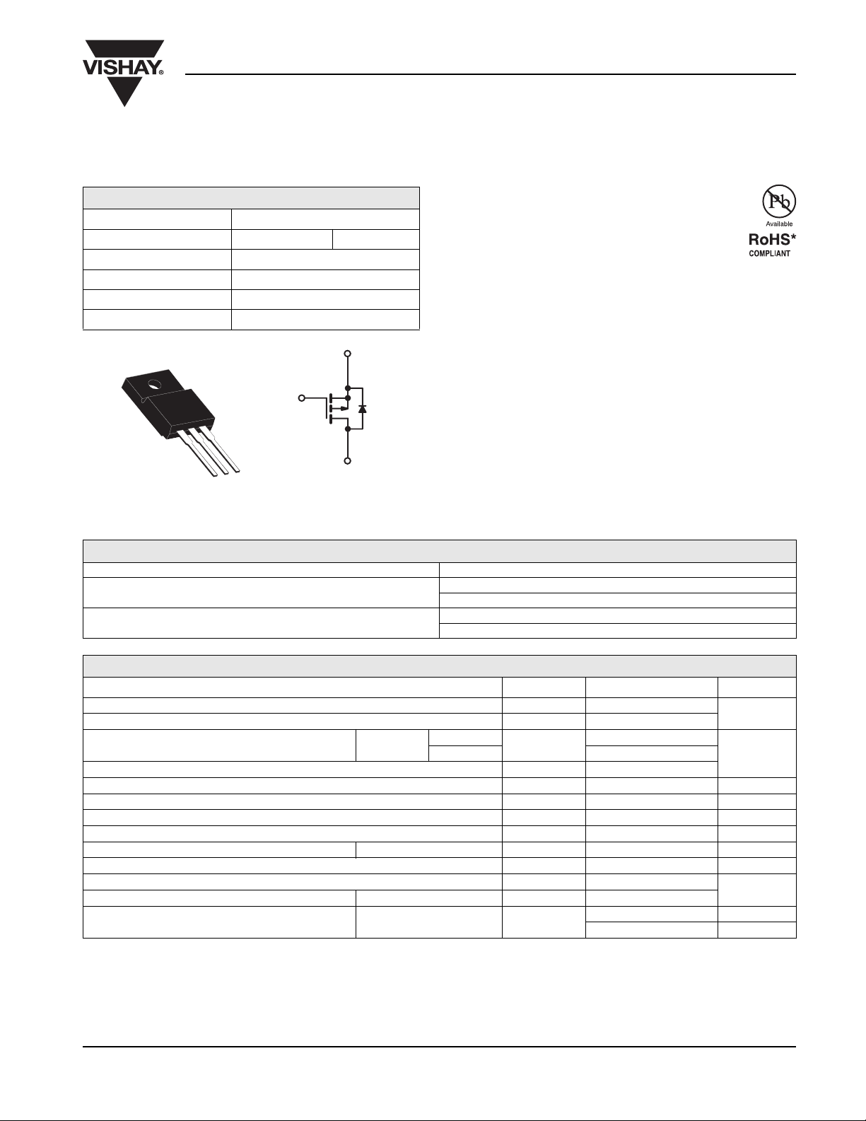
TO-220 FULLPAK
= - 10 V 1.0
GS
S
FEATURES
• Advanced Process Technology
• Dynamic dV/dt Rating
• 150 °C Operating Temperature
• Fast Switching
• P-Channel
• Fully Avalanche Rated
• Lead (Pb)-free Available
DESCRIPTION
Third generation Power MOSFETs from Vishay provide the
designer with the best combination of fast switching,
G
ruggedized device design, low on-resistance and
cost-effectiveness.
The TO-220 FULLPAK eliminates the need for additional
insulating hardware in commercial-industrial applications.
The moulding compound used provides a high isolation
S
D
G
D
P-Channel MOSFET
capability and a low thermal resistance between the tab and
external heatsink. This isolation is equivalent to using a 100
micron mica barrier with standard TO-220 product. The
FULLPAK is mounted to a heatsink using a single clip or by
a single screw fixing.
ORDERING INFORMATION
Package TO-220 FULLPAK
Lead (Pb)-free
SnPb
IRFI9634GPbF
SiHFI9634G-E3
IRFI9634G
SiHFI9634G
ABSOLUTE MAXIMUM RATINGS TC = 25 °C, unless otherwise noted
PARAMETER SYMBOL LIMIT UNIT
Drain-Source Voltage V
Gate-Source Voltage V
T
= 25 °C
Continuous Drain Current V
Pulsed Drain Current
a
at - 10 V
GS
C
= 100 °C - 2.6
T
C
DS
± 20
GS
I
D
IDM - 16
Linear Derating Factor 0.28 W/°C
Single Pulse Avalanche Energy
Repetitive Avalanche Current
Repetitive Avalanche Energy
Maximum Power Dissipation T
Peak Diode Recovery dV/dt
b
a
a
= 25 °C P
c
C
Operating Junction and Storage Temperature Range T
E
AS
I
AR
E
AR
D
dV/dt - 5.0 V/ns
, T
J
stg
Soldering Recommendations (Peak Temperature) for 10 s 300
Mounting Torque 6-32 or M3 screw
Notes
a. Repetitive rating; pulse width limited by maximum junction temperature (see fig. 11).
b. Starting T
c. I
SD
d. 1.6 mm from case.
= 25 °C, L = 62 mH, RG = 25 Ω, IAS = - 4.1 A (see fig. 12).
J
≤ - 4.1 A, dI/dt ≤ - 640 A/µs, VDD ≤ VDS, TJ ≤ 150 °C.
* Pb containing terminations are not RoHS compliant, exemptions may apply
Document Number: 91168 www.vishay.com
S09-0062-Rev. A, 02-Feb-09 1
- 250
- 4.1
520 mJ
- 4.1 A
3.5 mJ
35 W
- 55 to + 150
d
10 lbf · in
1.1 N · m
V
A
°C
IRFI9634G, SiHFI9634G
Vishay Siliconix
THERMAL RESISTANCE RATINGS
PARAMETER SYMBOL TYP. MAX. UNIT
Maximum Junction-to-Ambient R
Maximum Junction-to-Case (Drain) R
thJA
thJC
SPECIFICATIONS TJ = 25 °C, unless otherwise noted
PARAMETER SYMBOL TEST CONDITIONS MIN. TYP. MAX. UNIT
Static
Drain-Source Breakdown Voltage V
V
Temperature Coefficient ΔVDS/TJ Reference to 25 °C, ID = 1 mA - - 0.27 - V/°C
DS
Gate-Source Threshold Voltage V
Gate-Source Leakage I
Zero Gate Voltage Drain Current I
Drain-Source On-State Resistance R
Forward Transconductance g
Dynamic
Input Capacitance C
Output Capacitance C
Reverse Transfer Capacitance C
Drain to Sink Capacitance C f = 1.0 MHz - 12 -
Total Gate Charge Q
Gate-Drain Charge Q
Turn-On Delay Time t
Rise Time t
Turn-Off Delay Time t
Fall Time t
Internal Drain Inductance L
Internal Source Inductance L
Drain-Source Body Diode Characteristics
Continuous Source-Drain Diode Current I
Pulsed Diode Forward Current
a
Body Diode Voltage V
Body Diode Reverse Recovery Time t
Body Diode Reverse Recovery Charge Q
Forward Turn-On Time t
Notes
a. Repetitive rating; pulse width limited by maximum junction temperature (see fig. 11).
b. Pulse width ≤ 300 µs; duty cycle ≤ 2 %.
DS
GS(th)
V
GSS
DSS
DS(on)
fs
iss
- 170 -
oss
-40-
rss
g
--8.0
gs
--18
gd
d(on)
r
-34-
d(off)
-21-
f
D
V
DS
VGS = - 10 V ID = - 2.5 A
V
GS
Between lead,
6 mm (0.25") from
package and center of
S
S
I
SM
SD
rr
rr
on
die contact
MOSFET symbol
showing the
integral reverse
p - n junction diode
TJ = 25 °C, IS = - 4.1 A, VGS = 0 V
TJ = 25 °C, IF = - 4.1 A, dI/dt = -100 A/µs
-65
-3.6
°C/W
VGS = 0 V, ID = 250 µA - 250 - - V
VDS = VGS, ID = 250 µA - 2.0 - - 4.0 V
= ± 20 V - - ± 100 nA
GS
VDS = - 250 V, VGS = 0 V - - - 25
= - 200 V, VGS = 0 V, TJ = 150 °C - - - 250
VDS = - 50 V, ID = - 4.1 A
VGS = 0 V,
V
= - 25 V,
DS
f = 1.0 MHz, see fig. 5
b
b
--1.0Ω
2.2 - - S
- 680 -
--38
= - 4.1 A, VDS = - 200 V,
I
= - 10 V
D
see fig. 6 and 13
b
-12-
V
= - 130 V, ID = - 4.1 A,
DD
R
= 12 Ω, RD= 31 Ω,
G
see fig. 10
b
D
G
S
D
G
S
b
-23-
-4.5-
-7.5-
--- 4.1
--- 16
--- 6.5V
- 190 290 ns
b
-1.52.2µC
Intrinsic turn-on time is negligible (turn-on is dominated by LS and LD)
µA
pF
nC Gate-Source Charge Q
ns
nH
A
www.vishay.com Document Number: 91168
2 S09-0062-Rev. A, 02-Feb-09
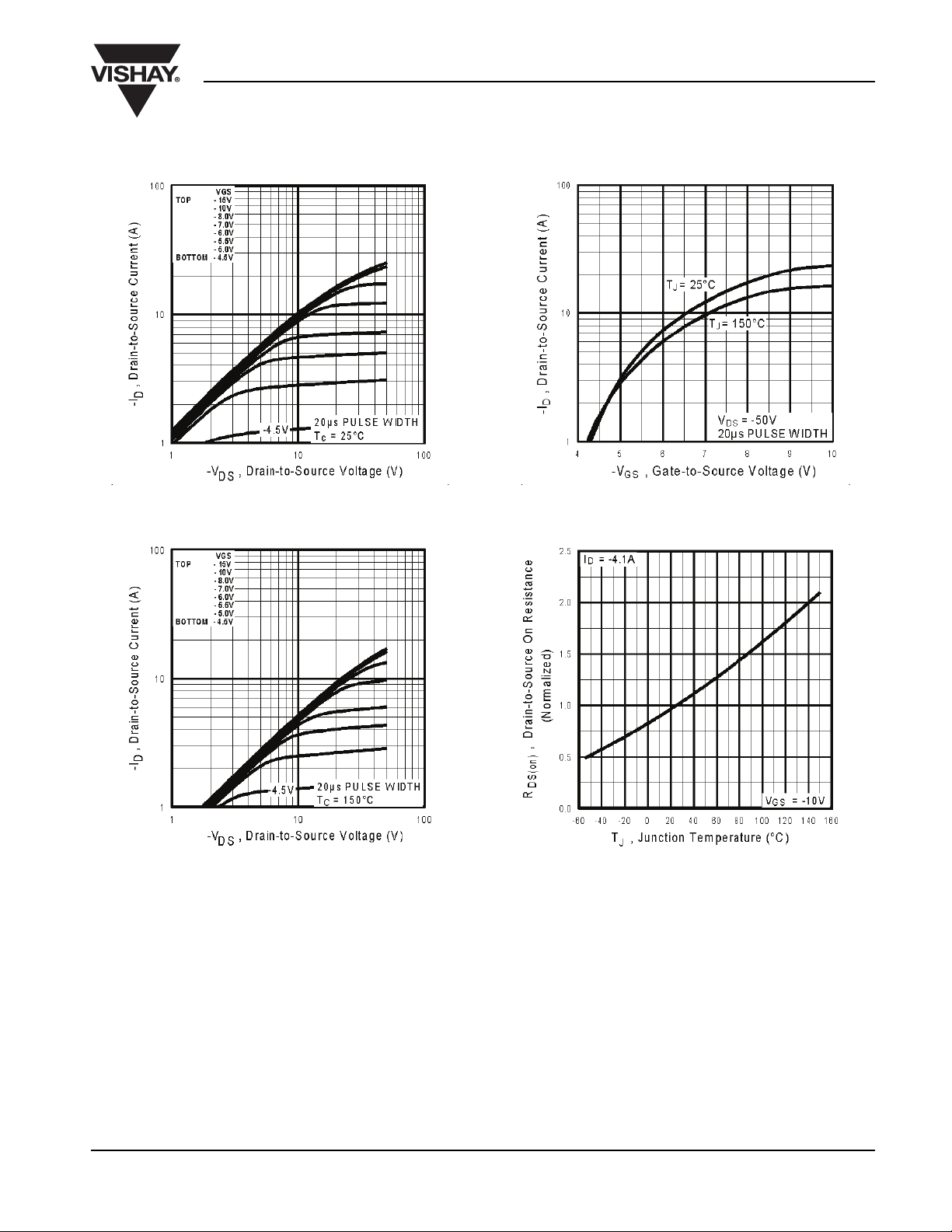
TYPICAL CHARACTERISTICS 25 °C, unless otherwise noted
IRFI9634G, SiHFI9634G
Vishay Siliconix
Fig. 1 - Typical Output Characteristics, TC = 25 °C
Fig. 2 - Typical Output Characteristics, T
= 150 °C
C
Fig. 3 - Typical Transfer Characteristics
Fig. 4 - Normalized On-Resistance vs. Temperature
Document Number: 91168 www.vishay.com
S09-0062-Rev. A, 02-Feb-09 3
 Loading...