

Power MOSFET
IRFI730G, SiHFI730G
Vishay Siliconix
PRODUCT SUMMARY
VDS (V) 400
(Ω)V
R
DS(on)
Q
(Max.) (nC) 38
g
Q
(nC) 5.7
gs
Q
(nC) 22
gd
Configuration Single
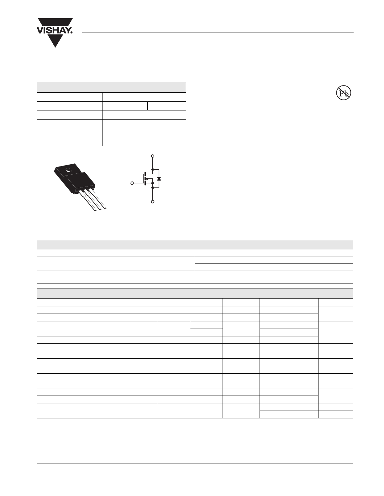
TO-220 FULLPAK
= 10 V 1.0
GS
D
FEATURES
• Isolated Package
• High Voltage Isolation = 2.5 kV
f = 60 Hz)
• Sink to Lead Creepage Distance = 4.8 mm
• Dynamic dV/dt Rating
• Low Thermal Resistance
• Lead (Pb)-free Available
DESCRIPTION
Third generation Power MOSFETs from Vishay provide the
designer with the best combination of fast switching,
ruggedized device design, low on-resistance and
G
cost-effectiveness.
The TO-220 FULLPAK eliminates the need for additional
insulating hardware in commercial-industrial applications.
The molding compound used provides a high isolation
S
D
G
N-Channel MOSFET
S
capability and a low thermal resistance between the tab and
external heatsink. This isolation is equivalent to using a 100
micron mica barrier with standard TO-220 product. The
FULLPAK is mounted to a heatsink using a single clip or by
a single screw fixing.
ORDERING INFORMATION
Package TO-220 FULLPAK
Lead (Pb)-free
SnPb
IRFI730GPbF
SiHFI730G-E3
IRFI730G
SiHFI730G
(t = 60 s;
RMS
Available
RoHS*
COMPLIANT
ABSOLUTE MAXIMUM RATINGS TC = 25 °C, unless otherwise noted
PARAMETER SYMBOL LIMIT UNIT
Drain-Source Voltage V
Gate-Source Voltage V
T
= 25 °C
Continuous Drain Current V
Pulsed Drain Current
a
at 10 V
GS
C
= 100 °C 2.3
C
DS
± 20
GS
I
D
IDM 15
Linear Derating Factor 0.28 W/°C
Single Pulse Avalanche Energy
Repetitive Avalanche Current
Repetitive Avalanche Energy
Maximum Power Dissipation T
Peak Diode Recovery dV/dt
Operating Junction and Storage Temperature Range T
b
a
a
= 25 °C P
c
C
E
AS
I
AR
E
AR
D
dV/dt 4.0 V/ns
, T
J
stg
Soldering Recommendations (Peak Temperature) for 10 s 300
Mounting Torque 6-32 or M3 screw
Notes
a. Repetitive rating; pulse width limited by maximum junction temperature (see fig. 11).
b. V
= 50 V, starting TJ = 25 °C, L = 25 mH, RG = 25 Ω, IAS = 3.7 A (see fig. 12).
DD
c. I
≤ 3.7 A, dI/dt ≤ 90 A/µs, VDD ≤ VDS, TJ ≤ 150 °C.
SD
d. 1.6 mm from case.
* Pb containing terminations are not RoHS compliant, exemptions may apply
Document Number: 91153 www.vishay.com
S09-0012-Rev. A, 19-Jan-09 1
400
3.7
200 mJ
3.7 A
3.5 mJ
35 W
- 55 to + 150
d
10 lbf · in
1.1 N · m
V
AT
°C
IRFI730G, SiHFI730G
Vishay Siliconix
THERMAL RESISTANCE RATINGS
PARAMETER SYMBOL TYP. MAX. UNIT
Maximum Junction-to-Ambient R
Maximum Junction-to-Case (Drain) R
thJA
thJC
SPECIFICATIONS TJ = 25 °C, unless otherwise noted
PARAMETER SYMBOL TEST CONDITIONS MIN. TYP. MAX. UNIT
Static
Drain-Source Breakdown Voltage V
Temperature Coefficient ΔVDS/TJ Reference to 25 °C, ID = 1 mA - 0.54 - V/°C
V
DS
Gate-Source Threshold Voltage V
Gate-Source Leakage I
Zero Gate Voltage Drain Current I
Drain-Source On-State Resistance R
Forward Transconductance g
Dynamic
Input Capacitance C
Output Capacitance C
Reverse Transfer Capacitance C
Drain to Sink Capacitance C f = 1.0 MHz - 12 -
Total Gate Charge Q
Gate-Drain Charge Q
Turn-On Delay Time t
Rise Time t
Turn-Off Delay Time t
Fall Time t
Internal Drain Inductance L
Internal Source Inductance L
Drain-Source Body Diode Characteristics
Continuous Source-Drain Diode Current I
Pulsed Diode Forward Current
a
Body Diode Voltage V
Body Diode Reverse Recovery Time t
Body Diode Reverse Recovery Charge Q
Forward Turn-On Time t
Notes
a. Repetitive rating; pulse width limited by maximum junction temperature (see fig. 11).
b. Pulse width ≤ 300 µs; duty cycle ≤ 2 %.
DS
GS(th)
V
GSS
DSS
VGS = 10 V ID = 2.1 A
DS(on)
fs
iss
- 170 -
oss
-64-
rss
g
--5.7
gs
--22
gd
d(on)
r
-38-
d(off)
-14-
f
D
V
V
GS
Between lead,
6 mm (0.25") from
package and center of
S
S
I
SM
SD
rr
rr
on
die contact
MOSFET symbol
showing the
integral reverse
p - n junction diode
TJ = 25 °C, IF = 3.7 A, dI/dt = 100 A/µs
-65
-3.6
°C/W
VGS = 0 V, ID = 250 µA 400 - - V
VDS = VGS, ID = 250 µA 2.0 - 4.0 V
= ± 20 V - - ± 100 nA
GS
VDS = 400 V, VGS = 0 V - - 25
= 320 V, VGS = 0 V, TJ = 125 °C - - 250
DS
VDS = 50 V, ID = 2.1 A
VGS = 0 V,
V
= 25 V,
DS
f = 1.0 MHz, see fig. 5
b
b
--1.0Ω
3.6 - - S
- 700 -
--38
= 3.7 A, VDS = 320 V,
I
= 10 V
D
see fig. 6 and 13
b
-10-
V
=200 V, ID = 3.7 A,
DD
R
= 12 Ω, RD= 57 Ω,
G
see fig. 10
b
G
G
TJ = 25 °C, IS = 3.7 A, VGS = 0 V
D
S
D
S
b
-15-
-4.5-
-7.5-
--3.7
--15
--1.6V
- 260 530 ns
b
-1.22.2µC
Intrinsic turn-on time is negligible (turn-on is dominated by LS and LD)
µA
pF
nC Gate-Source Charge Q
ns
nH
A
www.vishay.com Document Number: 91153
2 S09-0012-Rev. A, 19-Jan-09
TYPICAL CHARACTERISTICS 25 °C, unless otherwise noted
IRFI730G, SiHFI730G
Vishay Siliconix
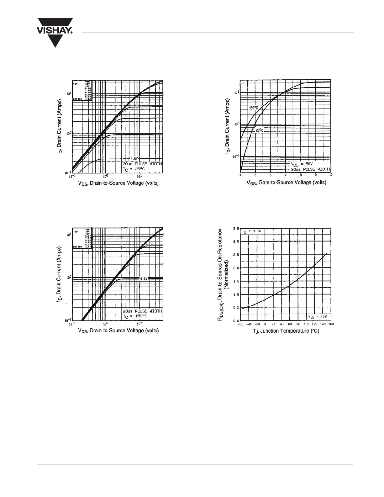
Fig. 1 - Typical Output Characteristics, TC = 25 °C
Fig. 2 - Typical Output Characteristics, T
= 150 °C
C
Fig. 3 - Typical Transfer Characteristics
Fig. 4 - Normalized On-Resistance vs. Temperature
Document Number: 91153 www.vishay.com
S09-0012-Rev. A, 19-Jan-09 3

IRFI730G, SiHFI730G
Vishay Siliconix
Fig. 5 - Typical Capacitance vs. Drain-to-Source Voltage
Fig. 6 - Typical Gate Charge vs. Gate-to-Source Voltage
Fig. 7 - Typical Source-Drain Diode Forward Voltage
Fig. 8 - Maximum Safe Operating Area
www.vishay.com Document Number: 91153
4 S09-0012-Rev. A, 19-Jan-09

Fig. 9 - Maximum Drain Current vs. Case Temperature
IRFI730G, SiHFI730G
Vishay Siliconix
R
D.U.T.
D
t
d(off)
+
-
t
f
V
DS
V
GS
R
G
10 V
Pulse width ≤ 1 µs
Duty factor ≤ 0.1 %
Fig. 10a - Switching Time Test Circuit
V
DS
90 %
10 %
V
GS
t
t
d(on)
r
Fig. 10b - Switching Time Waveforms
V
DD
Fig. 11 - Maximum Effective Transient Thermal Impedance, Junction-to-Case
to obtain
Vary t
p
required I
AS
V
L
DS
t
p
R
G
D.U.T
I
AS
+
V
DD
-
V
DS
V
DS
V
DD
10 V
t
p
0.01 Ω
I
AS
Fig. 12a - Unclamped Inductive Test Circuit Fig. 12b - Unclamped Inductive Waveforms
Document Number: 91153 www.vishay.com
S09-0012-Rev. A, 19-Jan-09 5

IRFI730G, SiHFI730G
Vishay Siliconix
Fig. 12c - Maximum Avalanche Energy vs. Drain Current
Q
10 V
V
Q
GS
G
G
Q
GD
Charge
Fig. 13a - Basic Gate Charge Waveform
Current regulator
Same type as D.U.T.
50 kΩ
0.2 µF
12 V
0.3 µF
D.U.T.
V
GS
3 mA
I
G
Current sampling resistors
I
D
Fig. 13b - Gate Charge Test Circuit
+
V
DS
-
www.vishay.com Document Number: 91153
6 S09-0012-Rev. A, 19-Jan-09
IRFI730G, SiHFI730G
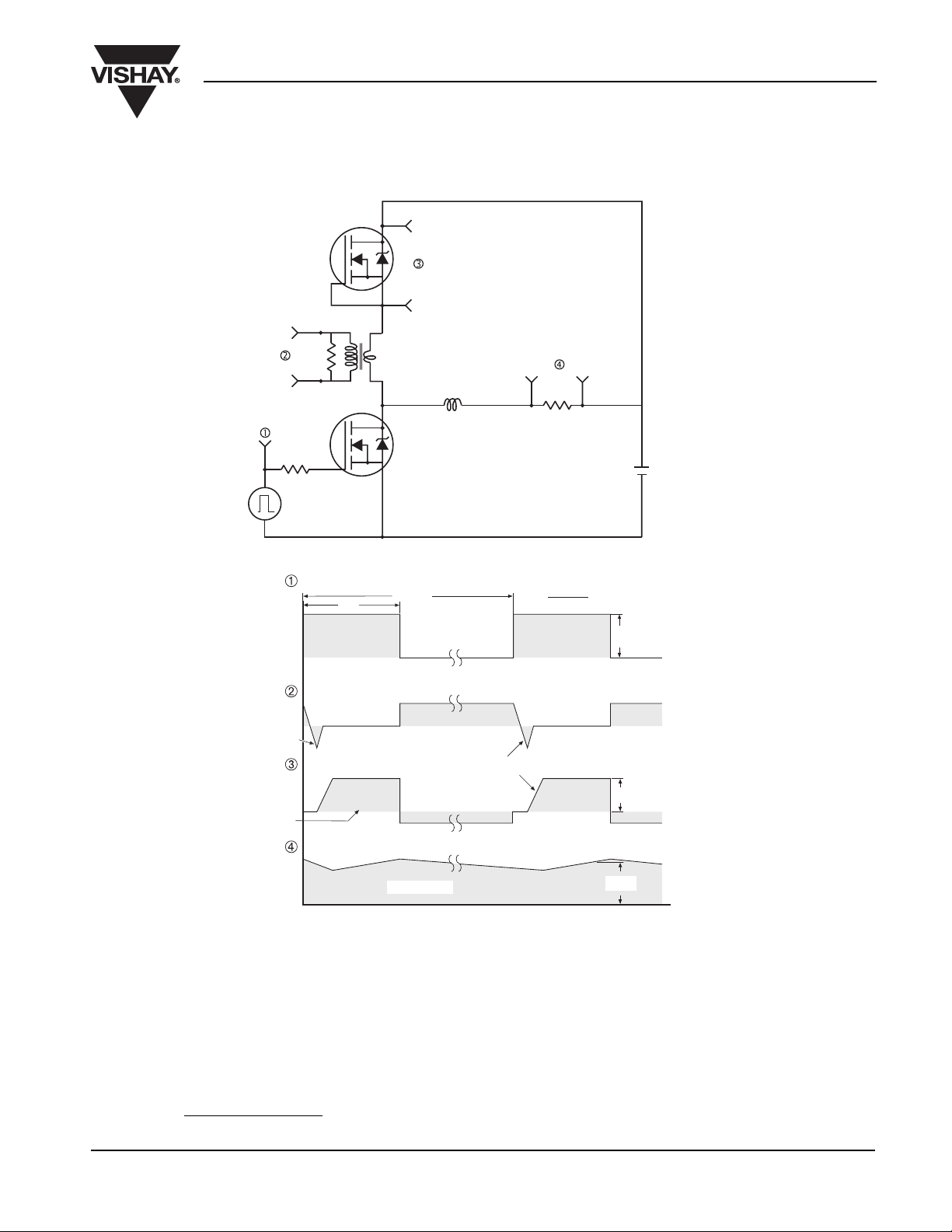
Peak Diode Recovery dV/dt Test Circuit
Vishay Siliconix
D.U.T.
+
-
R
G
Driver gate drive
P.W.
+
Circuit layout considerations
• Low stray inductance
• Ground plane
• Low leakage inductance
current transformer
-
• dV/dt controlled by R
• Driver same type as D.U.T.
• I
controlled by duty factor "D"
SD
• D.U.T. - device under test
Period
-
D =
G
P.W.
Period
+
+
V
DD
-
= 10 V*
V
GS
waveform
SD
Body diode forward
current
waveform
DS
Body diode forward drop
Ripple ≤ 5 %
= 5 V for logic level devices
GS
Diode recovery
dV/dt
dI/dt
V
DD
I
SD
Reverse
recovery
current
Re-applied
voltage
D.U.T. I
D.U.T. V
Inductor current
* V
Fig.14 - For N-Channel
Vishay Siliconix maintains worldwide manufacturing capability. Products may be manufactured at one of several qualified locations. Reliability data for Silicon
Technology and Package Reliability represent a composite of all qualified locations. For related documents such as package/tape drawings, part marking, and
reliability data, see www.vishay.com/ppg?91153
.
Document Number: 91153 www.vishay.com
S09-0012-Rev. A, 19-Jan-09 7

Legal Disclaimer Notice
www.vishay.com
Vishay
Disclaimer
ALL PRODUCT, PRODUCT SPECIFICATIONS AND DATA ARE SUBJECT TO CHANGE WITHOUT NOTICE TO IMPROVE
RELIABILITY, FUNCTION OR DESIGN OR OTHERWISE.
Vishay Intertechnology, Inc., its affiliates, agents, and employees, and all persons acting on its or their behalf (collectively,
“Vishay”), disclaim any and all liability for any errors, inaccuracies or incompleteness contained in any datasheet or in any other
disclosure relating to any product.
Vishay makes no warranty, representation or guarantee regarding the suitability of the products for any particular purpose or
the continuing production of any product. To the maximum extent permitted by applicable law, Vishay disclaims (i) any and all
liability arising out of the application or use of any product, (ii) any and all liability, including without limitation special,
consequential or incidental damages, and (iii) any and all implied warranties, including warranties of fitness for particular
purpose, non-infringement and merchantability.
Statements regarding the suitability of products for certain types of applications are based on Vishay’s knowledge of
typical requirements that are often placed on Vishay products in generic applications. Such statements are not binding
statements about the suitability of products for a particular application. It is the customer’s responsibility to validate that a
particular product with the properties described in the product specification is suitable for use in a particular application.
Parameters provided in datasheets and / or specifications may vary in different applications and performance may vary over
time. All operating parameters, including typical parameters, must be validated for each customer application by the customer’s
technical experts. Product specifications do not expand or otherwise modify Vishay’s terms and conditions of purchase,
including but not limited to the warranty expressed therein.
Except as expressly indicated in writing, Vishay products are not designed for use in medical, life-saving, or life-sustaining
applications or for any other application in which the failure of the Vishay product could result in personal injury or death.
Customers using or selling Vishay products not expressly indicated for use in such applications do so at their own risk.
Please contact authorized Vishay personnel to obtain written terms and conditions regarding products designed for
such applications.
No license, express or implied, by estoppel or otherwise, to any intellectual property rights is granted by this document
or by any conduct of Vishay. Product names and markings noted herein may be trademarks of their respective owners.
Revision: 13-Jun-16
1
Document Number: 91000
 Loading...