

Vishay IRFD420, SiHFD420 Data Sheet
Power MOSFET
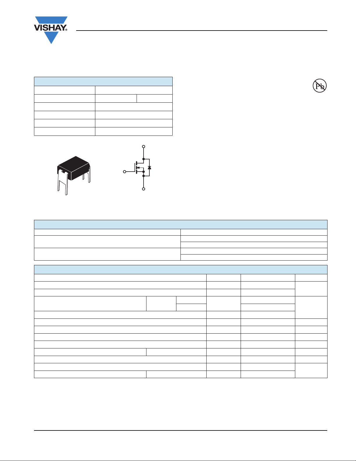
N-Channel MOSFET
G
D
S
HVMDIP
D
S
G
Available
RoHS*
COMPLIANT
IRFD420, SiHFD420
Vishay Siliconix
PRODUCT SUMMARY
VDS (V) 500
()V
R
DS(on)
Q
(Max.) (nC) 24
g
Q
(nC) 3.3
gs
Q
(nC) 13
gd
Configuration Single
= 10 V 3.0
GS
FEATURES
• Dynamic dV/dt Rating
• Repetitive Avalanche Rated
• For Automatic Insertion
•End Stackable
•Fast Switching
• Ease of Paralleling
• Simple Drive Requirements
• Compliant to RoHS Directive 2002/95/EC
DESCRIPTION
Third generation Power MOSFETs from Vishay provide the
designer with the best combination of fast switching,
ruggedized device design, low on-resistance and
cost-effectiveness.
The 4 pin DIP package is a low cost machine-insertable
case style which can be stacked in multiple combinations on
standard 0.1 inch pin centers. The dual drain serves as a
thermal link to the mounting surface for power dissipation
levels up to 1 W.
ORDERING INFORMATION
Package HVMDIP
Lead (Pb)-free
SnPb
IRFD420PbF
SiHFD420-E3
IRFD420
SiHFD420
ABSOLUTE MAXIMUM RATINGS (TA = 25 °C, unless otherwise noted)
PARAMETER SYMBOL LIMIT UNIT
Drain-Source Voltage V
Gate-Source Voltage V
T
= 25 °C
Continuous Drain Current V
Pulsed Drain Current
a
at 10 V
GS
A
= 100 °C 0.23
A
DS
± 20
GS
I
D
IDM 3.0
Linear Derating Factor 0.0083 W/°C
Single Pulse Avalanche Energy
Repetitive Avalanche Current
Repetitive Avalanche Energy
Maximum Power Dissipation T
Peak Diode Recovery dV/dt
Operating Junction and Storage Temperature Range T
b
a
a
= 25 °C P
c
A
E
AS
I
AR
E
AR
D
dV/dt 3.5 V/ns
, T
J
stg
Soldering Recommendations (Peak Temperature) for 10 s 300
Notes
a. Repetitive rating; pulse width limited by maximum junction temperature.
= 50 V, starting TJ = 25 °C, L = 40 mH, Rg = 25 , IAS = 1.5 A.
b. V
DD
c. I
4.4 A, dI/dt 90 A/μs, VDD VDS, TJ 150 °C.
SD
d. 1.6 mm from case.
* Pb containing terminations are not RoHS compliant, exemptions may apply
Document Number: 91135 www.vishay.com
S10-2463-Rev. C, 08-Nov-10 1
500
0.37
51 mJ
0.37 A
0.10 mJ
1.0 W
- 55 to + 150
d
V
AT
°C
IRFD420, SiHFD420
Vishay Siliconix
THERMAL RESISTANCE RATINGS
PARAMETER SYMBOL TYP. MAX. UNIT
Maximum Junction-to-Ambient R
thJA
SPECIFICATIONS (TJ = 25 °C, unless otherwise noted)
PARAMETER SYMBOL TEST CONDITIONS MIN. TYP. MAX. UNIT
Static
Drain-Source Breakdown Voltage V
V
Temperature Coefficient VDS/TJ Reference to 25 °C, ID = 1 mA - 0.59 - V/°C
DS
Gate-Source Threshold Voltage V
Gate-Source Leakage I
Zero Gate Voltage Drain Current I
Drain-Source On-State Resistance R
Forward Transconductance g
Dynamic
Input Capacitance C
Reverse Transfer Capacitance C
Total Gate Charge Q
Gate-Drain Charge Q
Turn-On Delay Time t
Rise Time t
Turn-Off Delay Time t
Fall Time t
Internal Drain Inductance L
Internal Source Inductance L
Drain-Source Body Diode Characteristics
Continuous Source-Drain Diode Current I
Pulsed Diode Forward Current
a
Body Diode Voltage V
Body Diode Reverse Recovery Time t
Body Diode Reverse Recovery Charge Q
Forward Turn-On Time t
Notes
a. Repetitive rating; pulse width limited by maximum junction temperature (see fig. 11).
b. Pulse width 300 μs; duty cycle 2 %.
DS
GS(th)
V
GSS
DSS
VGS = 10 V ID = 0.22 A
DS(on)
fs
iss
-92-
oss
-37-
rss
g
--3.3
gs
--13
gd
d(on)
r
-33-
d(off)
-16-
f
D
V
V
GS
Between lead,
6 mm (0.25") from
package and center of
S
S
die contact
MOSFET symbol
showing the
integral reverse
I
SM
SD
rr
rr
on
p - n junction diode
TJ = 25 °C, IS = 0.37 A, VGS = 0 V
TJ = 25 °C, IF = 2.1 A, dI/dt = 100 A/μs
- 120 °C/W
VGS = 0 V, ID = 250 μA 500 - - V
VDS = VGS, ID = 250 μA 2.0 - 4.0 V
= ± 20 V - - ± 100 nA
GS
VDS = 500 V, VGS = 0 V - - 25
= 400 V, VGS = 0 V, TJ = 125 °C - - 250
DS
VDS = 50 V, ID = 1.3 A
VGS = 0 V,
V
= 25 V,
DS
f = 1.0 MHz
b
b
--3.0
1.5 - - S
- 360 -
--24
= 10 V ID = 2.1 A, VDS = 400 V
b
-8.0-
V
= 250 V, ID = 2.1 A,
DD
R
= 18 , RD = 120
g
b
D
G
S
D
G
S
b
-8.6-
-4.0-
-6.0-
- - 0.37
--5.0
--1.6V
- 260 520 ns
b
- 0.70 1.4 μC
Intrinsic turn-on time is negligible (turn-on is dominated by LS and LD)
μA
pFOutput Capacitance C
nC Gate-Source Charge Q
ns
nH
A
www.vishay.com Document Number: 91135
2 S10-2463-Rev. C, 08-Nov-10
TYPICAL CHARACTERISTICS (25 °C, unless otherwise noted)
TA = 25 °C
TA = 150 °C
IRFD420, SiHFD420
Vishay Siliconix
Fig. 1 - Typical Output Characteristics, TA = 25 °C
Fig. 2 - Typical Output Characteristics, T
= 150 °C
A
Fig. 3 - Typical Transfer Characteristics
Fig. 4 - Normalized On-Resistance vs. Temperature
Document Number: 91135 www.vishay.com
S10-2463-Rev. C, 08-Nov-10 3
 Loading...