

Page 1
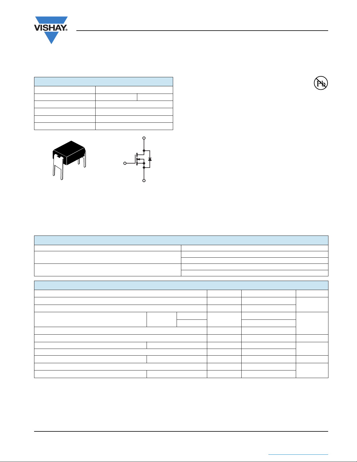
N-Channel MOSFET
G
D
S
HVMDIP
D
S
G
Available
RoHS*
COMPLIANT
Power MOSFET
IRFD020, SiHFD020
Vishay Siliconix
PRODUCT SUMMARY
VDS (V) 50
R
()V
DS(on)
Q
(Max.) (nC) 24
g
Q
(nC) 7.1
gs
Q
(nC) 7.1
gd
Configuration Single
= 10 V 0.10
GS
FEATURES
• For Automatic Insertion
• Compact, End Stackable
•Fast Switching
• Ease of Paralleling
• Excellent Temperature Stability
• Compliant to RoHS Directive 2002/95/EC
DESCRIPTION
The HVMDIP technology is the key to Vishay’s advanced
line of power MOSFET transistors. The efficient geometry
and unique processing of the HVMDIP design achieves
very low on-state resistance combined with high
transconductance and extreme device ruggedness.
HVMDIPs feature all of the established advantages of
MOSFETs such as voltage control, very fast switching, ease
of paralleling, and temperature stability of the electrical
parameters.
The HVMDIP 4 pin, dual-in-line package brings the
advantages of HVMDIPs to high volume applications where
automatic PC board insertion is desireable, such as circuit
boards for computers, printers, telecommunications
equipment, and consumer products. Their compatibility with
automatic insertion equipment, low-profile and end
stackable features represent the stat-of-the-art in power
device packaging.
ORDERING INFORMATION
Package HVMDIP
Lead (Pb)-free
SnPb
IRFD020PbF
SiHFD020-E3
IRFD020
SiHFD020
ABSOLUTE MAXIMUM RATINGS (TC = 25 °C, unless otherwise noted)
PARAMETER SYMBOL LIMIT UNIT
Drain-Source Voltage
Gate-Source Voltage V
Continuous Drain Current V
Pulsed Drain Current
Linear Derating Factor 0.0080 W/°C
Inductive Current, Clamped L = 100 μH I
Unclamped Inductive Current (Avalanche Current)
Maximum Power Dissipation T
Operating Junction and Storage Temperature Range T
Soldering Recommendations (Peak Temperature) for 10 s 300
Notes
a. T
= 25 °C to 150 °C
J
b. Repetitive rating; pulse width limited by maximum junction temperature.
c. V
= 25 V, starting TJ = 25 °C, L = 100 μH, Rg = 25
DD
d. 1.6 mm from case.
* Pb containing terminations are not RoHS compliant, exemptions may apply
Document Number: 91465 www.vishay.com
S11-0915-Rev. A, 16-May-11 1
THE PRODUCTS DESCRIBED HEREIN AND THIS DOCUMENT ARE SUBJECT TO SPECIFIC DISCLAIMERS, SET FORTH AT
a
T
= 25 °C
at 10 V
GS
b
c
This document is subject to change without notice.
C
= 100 °C 1.5
C
= 25 °C P
C
V
DS
± 20
GS
I
D
IDM 19
LM
I
L
D
, T
J
stg
- 55 to + 150
50
2.4
19
2.2
1.0 W
d
www.vishay.com/doc?91000
V
AT
A
°C
Page 2
IRFD020, SiHFD020
Vishay Siliconix
THERMAL RESISTANCE RATINGS
PARAMETER SYMBOL TYP. MAX. UNIT
Maximum Junction-to-Ambient R
thJA
SPECIFICATIONS (TC = 25 °C, unless otherwise noted)
PARAMETER SYMBOL TEST CONDITIONS MIN. TYP. MAX. UNIT
Static
Drain-Source Breakdown Voltage V
Gate-Source Threshold Voltage V
Gate-Source Leakage I
Zero Gate Voltage Drain Current I
On-State Drain Current
Drain-Source On-State Resistance
Forward Transconductance
b
b
R
b
Dynamic
Input Capacitance C
Reverse Transfer Capacitance C
Total Gate Charge Q
Gate-Drain Charge Q
Turn-On Delay Time t
Rise Time t
Turn-Off Delay Time t
Fall Time t
Internal Drain Inductance L
Internal Source Inductance L
Drain-Source Body Diode Characteristics
Continuous Source-Drain Diode Current I
Pulsed Diode Forward Current
Body Diode Voltage
a
c
Body Diode Reverse Recovery Time t
Body Diode Reverse Recovery Charge Q
Forward Turn-On Time t
Notes
a. Repetitive rating; pulse width limited by maximum junction temperature (see fig. 11).
b. Pulse width 300 μs; duty cycle 2 %.
c. V
= 25 V, starting TJ = 25 °C, L = 100 μH, Rg = 25
DD
DS
GS(th)
V
GSS
DSS
I
V
D(on)
VGS = 10 V ID = 1.4 A - 0.080 0.10
DS(on)
g
fs
iss
- 260 -
oss
-44-
rss
g
-4.77.1
gs
-4.77.1
gd
d(on)
r
-1624
d(off)
-2639
f
D
= max. rating x 0.8, VGS = 0 V, TC = 125
V
DS
GS
V
GS
Between lead,
6 mm (0.25") from
package and center of
S
S
die contact
MOSFET symbol
showing the
integral reverse
I
SM
V
SD
rr
rr
on
p - n junction diode
TJ = 25 °C, IF = 15 A, dI/dt = 100 A/μs
- 120 °C/W
VGS = 0 V, ID = 250 μA 50 - - V
VDS = VGS, ID = 250 μA 2.0 - 4.0 V
= ± 20 V - - ± 500 nA
GS
VDS = max. rating, VGS = 0 V - - 250
- - 1000
= 10 V VDS > I
D(on)
x R
max. 2.4 - - A
DS(on)
VDS = 20 V, ID = 7.5 A 4.9 7.3 - S
VGS = 0 V,
V
= 25 V,
DS
f = 1.0 MHz
- 400 -
-1624
= 15 A,
I
= 10 V
D
V
= max. rating x 0.8
DS
-8.713
V
= 25 V, ID = 15 A,
DD
R
= 18 , RD = 1.7
g
D
G
S
D
G
S
-5583
-4.0-
-6.0-
--2.4
--19
TC = 25 °C, IS = 2.4 A, VGS = 0 V - - 1.4 V
57 130 310 ns
0.17 0.34 0.85 μC
Intrinsic turn-on time is negligible (turn-on is dominated by LS and LD)
μA
pFOutput Capacitance C
nC Gate-Source Charge Q
ns
nH
A
www.vishay.com Document Number: 91465
2 S11-0915-Rev. A, 16-May-11
This document is subject to change without notice.
THE PRODUCTS DESCRIBED HEREIN AND THIS DOCUMENT ARE SUBJECT TO SPECIFIC DISCLAIMERS, SET FORTH AT
www.vishay.com/doc?91000
Page 3
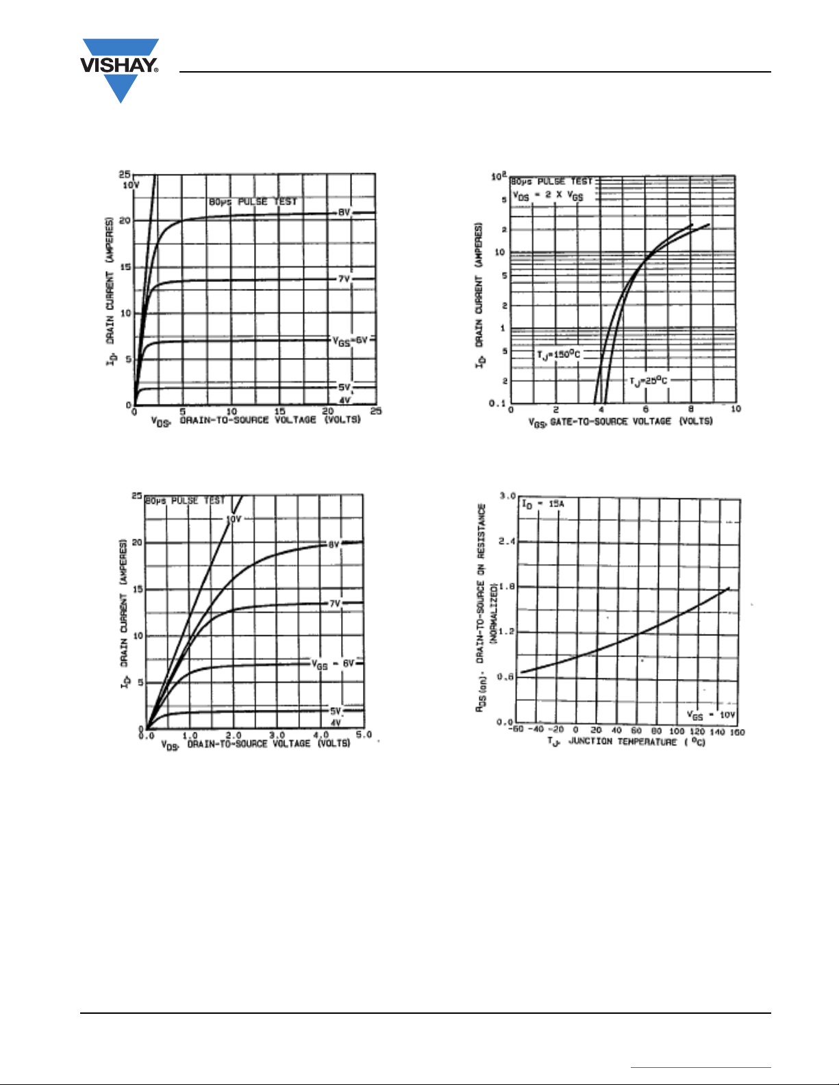
TYPICAL CHARACTERISTICS (25 °C, unless otherwise noted)
IRFD020, SiHFD020
Vishay Siliconix
Fig. 1 - Typical Output Characteristics
Fig. 2 - Typical Output Characteristics
Fig. 3 - Typical Transfer Characteristics
Fig. 4 - Normalized On-Resistance vs. Temperature
Document Number: 91465 www.vishay.com
S11-0915-Rev. A, 16-May-11 3
THE PRODUCTS DESCRIBED HEREIN AND THIS DOCUMENT ARE SUBJECT TO SPECIFIC DISCLAIMERS, SET FORTH AT
This document is subject to change without notice.
www.vishay.com/doc?91000
Page 4

IRFD020, SiHFD020
Vishay Siliconix
Fig. 5 - Typical Capacitance vs. Drain-to-Source Voltage
Fig. 6 - Typical Gate Charge vs. Gate-to-Source Voltage
Fig. 7 - Typical Source-Drain Diode Forward Voltage
Fig. 8 - Maximum Safe Operating Area
www.vishay.com Document Number: 91465
4 S11-0915-Rev. A, 16-May-11
THE PRODUCTS DESCRIBED HEREIN AND THIS DOCUMENT ARE SUBJECT TO SPECIFIC DISCLAIMERS, SET FORTH AT
This document is subject to change without notice.
www.vishay.com/doc?91000
Page 5

IRFD020, SiHFD020
Vishay Siliconix
Fig. 9 - Maximum Drain Current vs. Ambient Temperature
Fig. 10 - Maximum Effective Transient Thermal Impedance, Junction-to-Ambient
Fig. 11 - Typical Transconductance vs. Drain Current Fig. 12 - Breakdown Voltage vs. Temperature
Document Number: 91465 www.vishay.com
S11-0915-Rev. A, 16-May-11 5
THE PRODUCTS DESCRIBED HEREIN AND THIS DOCUMENT ARE SUBJECT TO SPECIFIC DISCLAIMERS, SET FORTH AT
This document is subject to change without notice.
www.vishay.com/doc?91000
Page 6

IRFD020, SiHFD020
Vishay Siliconix
Fig. 15a - Unclamped Inductive Load Test Waveforms
Fig. 13 - Typical on-Resistance vs. Drain Current
Fig. 14a - Clamped Inductive Test Circuit
Fig. 14b - Clamped Inductive Waveforms
Fig. 16 - Switching Time Test Circuit
Fig. 17 - Gate Charge Test Circuit
Fig. 15a - Unclamped Inductive Test Circuit
www.vishay.com Document Number: 91465
6 S11-0915-Rev. A, 16-May-11
THE PRODUCTS DESCRIBED HEREIN AND THIS DOCUMENT ARE SUBJECT TO SPECIFIC DISCLAIMERS, SET FORTH AT
This document is subject to change without notice.
www.vishay.com/doc?91000
Page 7

IRFD020, SiHFD020
Vishay Siliconix
Fig. 18 - Typical Time to Accumulated 1 % Gate Failure Fig. 19 - Typical High Temperature Reverse Bias (HTRB) Failure
Rate
Vishay Siliconix maintains worldwide manufacturing capability. Products may be manufactured at one of several qualified locations. Reliability data for Silicon
Technology and Package Reliability represent a composite of all qualified locations. For related documents such as package/tape drawings, part marking, and
reliability data, see www.vishay.com/ppg?91465
Document Number: 91465 www.vishay.com
S11-0915-Rev. A, 16-May-11 7
THE PRODUCTS DESCRIBED HEREIN AND THIS DOCUMENT ARE SUBJECT TO SPECIFIC DISCLAIMERS, SET FORTH AT
.
This document is subject to change without notice.
www.vishay.com/doc?91000
Page 8

HVM DIP (High voltage)
Package Information
Vishay Siliconix
0.248 [6.29]
0.240 [6.10]
0.043 [1.09]
0.035 [0.89]
0.094 [2.38]
0.086 [2.18]
0.017 [0.43]
0.013 [0.33]
0° to 15°
2 x
E min.
E max.
0.133 [3.37]
0.125 [3.18]
0.045 [1.14]
2 x
0.035 [0.89]
A
0.100 [2.54] typ.
L
0.197 [5.00]
0.189 [4.80]
0.160 [4.06]
0.140 [3.56]
0.024 [0.60]
0.020 [0.51]
0.180 [4.57]
0.160 [4.06]
4 x
INCHES MILLIMETERS
DIM. MIN. MAX. MIN. MAX.
A 0.310 0.330 7.87 8.38
E 0.300 0.425 7.62 10.79
L 0.270 0.290 6.86 7.36
ECN: X10-0386-Rev. B, 06-Sep-10
DWG: 5974
Note
1. Package length does not include mold flash, protrusions or gate burrs. Package width does not include interlead flash or protrusions.
Document Number: 91361 www.vishay.com
Revision: 06-Sep-10 1
Page 9

Legal Disclaimer Notice
www.vishay.com
Vishay
Disclaimer
ALL PRODUCT, PRODUCT SPECIFICATIONS AND DATA ARE SUBJECT TO CHANGE WITHOUT NOTICE TO IMPROVE
RELIABILITY, FUNCTION OR DESIGN OR OTHERWISE.
Vishay Intertechnology, Inc., its affiliates, agents, and employees, and all persons acting on its or their behalf (collectively,
“Vishay”), disclaim any and all liability for any errors, inaccuracies or incompleteness contained in any datasheet or in any other
disclosure relating to any product.
Vishay makes no warranty, representation or guarantee regarding the suitability of the products for any particular purpose or
the continuing production of any product. To the maximum extent permitted by applicable law, Vishay disclaims (i) any and all
liability arising out of the application or use of any product, (ii) any and all liability, including without limitation special,
consequential or incidental damages, and (iii) any and all implied warranties, including warranties of fitness for particular
purpose, non-infringement and merchantability.
Statements regarding the suitability of products for certain types of applications are based on Vishay’s knowledge of
typical requirements that are often placed on Vishay products in generic applications. Such statements are not binding
statements about the suitability of products for a particular application. It is the customer’s responsibility to validate that a
particular product with the properties described in the product specification is suitable for use in a particular application.
Parameters provided in datasheets and / or specifications may vary in different applications and performance may vary over
time. All operating parameters, including typical parameters, must be validated for each customer application by the customer’s
technical experts. Product specifications do not expand or otherwise modify Vishay’s terms and conditions of purchase,
including but not limited to the warranty expressed therein.
Except as expressly indicated in writing, Vishay products are not designed for use in medical, life-saving, or life-sustaining
applications or for any other application in which the failure of the Vishay product could result in personal injury or death.
Customers using or selling Vishay products not expressly indicated for use in such applications do so at their own risk.
Please contact authorized Vishay personnel to obtain written terms and conditions regarding products designed for
such applications.
No license, express or implied, by estoppel or otherwise, to any intellectual property rights is granted by this document
or by any conduct of Vishay. Product names and markings noted herein may be trademarks of their respective owners.
Revision: 13-Jun-16
1
Document Number: 91000
 Loading...