

Page 1
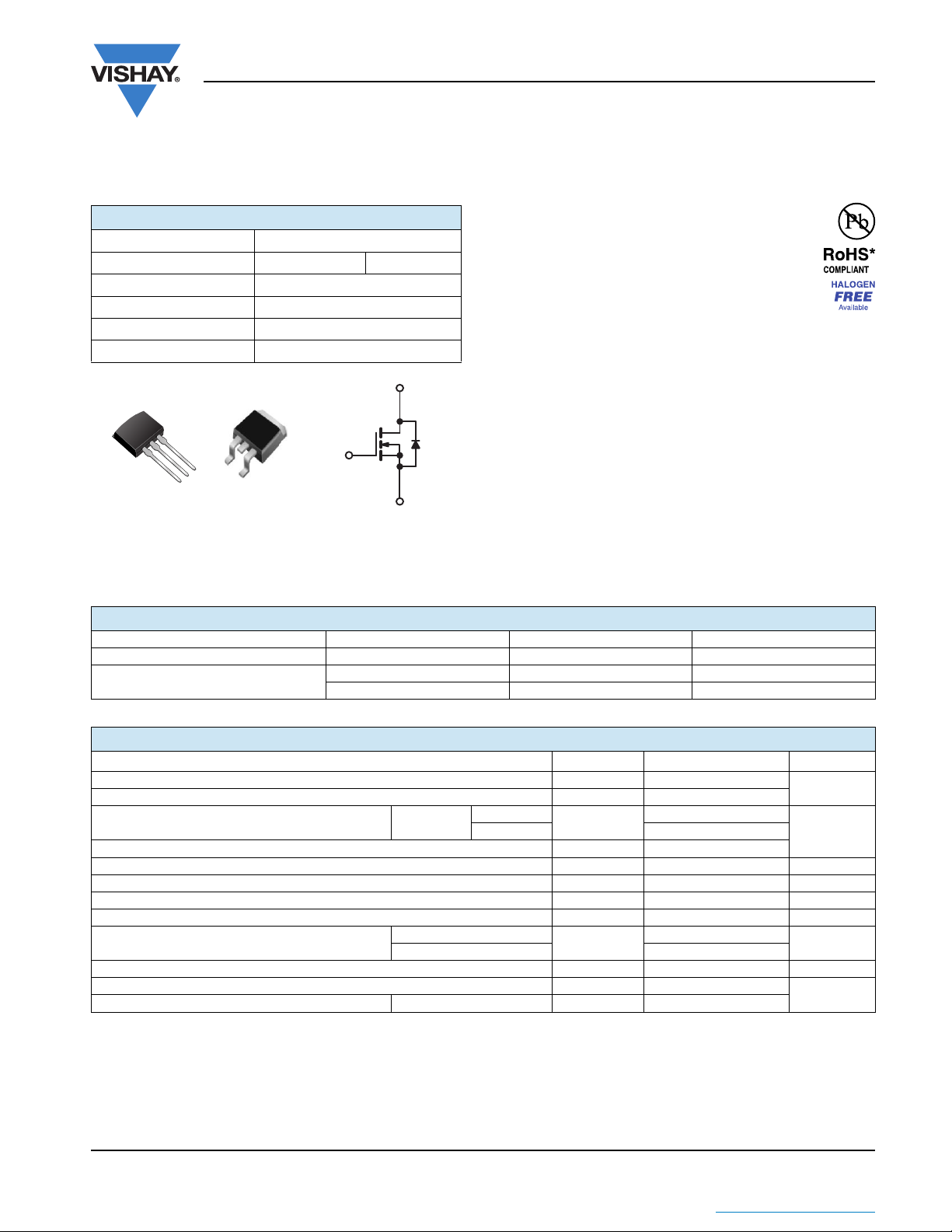
D2PAK (TO-263)
G
D
S
I2PAK (TO-262)
G
D
S
IRFBC30S, SiHFBC30S, IRFBC30L, SiHFBC30L
Vishay Siliconix
Power MOSFET
PRODUCT SUMMARY
VDS (V) 600
()V
R
DS(on)
Q
(Max.) (nC) 31
g
Q
(nC) 4.6
gs
Q
(nC) 17
gd
Configuration Single
= 10 V 2.2
GS
D
FEATURES
• Halogen-free According to IEC 61249-2-21
Definition
• Surface Mount (IRFBC30S, SiHFBC30S)
• Low-Profile Through-Hole (IRFBC30L, SiHFBC30L)
•
Available in Tape and Reel (IRFBC30S, SiHFBC30S)
• Dynamic dV/dt Rating
• 150 °C Operating Temperature
•Fast Switching
• Fully Avalanche Rated
• Compliant to RoHS Directive 2002/95/EC
DESCRIPTION
Third generation Power MOSFETs from Vishay provide the
designer with the best combination of fast switching,
ruggedized device design, low on-resistance and
G
cost-effectiveness.
2
PAK is a surface mount power package capable of
The D
the accommodating die sizes up to HEX-4. It provides the
highest power capability and the lowest possible
S
N-Channel MOSFET
on-resistance in any existing surface mount package. The
D2PAK is suitable for high current applications because of
its low internal connection resistance and can dissipate up
to 2.0 W in a typical surface mount application. The
through-hole version (IRFBC30L, SiHFBC30L) is a available
for low-profile applications.
ORDERING INFORMATION
Package D2PAK (TO-263) D2PAK (TO-263) I2PAK (TO-262)
Lead (Pb)-free and Halogen-free SiHFBC30S-GE3 SiHFBC30STRL-GE3
Lead (Pb)-free
Note
a. See device orientation.
IRFBC30SPbF IRFBC30STRLPbF
SiHFBC30S-E3 SiHFBC30STL-E3
a
SiHFBC30L-GE3
a
IRFBC30LPbF
a
SiHFBC30L-E3
ABSOLUTE MAXIMUM RATINGS (TC = 25 °C, unless otherwise noted)
PARAMETER SYMBOL LIMIT UNIT
Drain-Source Voltage
Gate-Source Voltage
Continuous Drain Current
Pulsed Drain Current
a, e
= 25 °C
T
e
VGS at 10 V
C
T
= 100 °C
C
V
DS
V
GS
I
D
IDM
Linear Derating Factor 0.59 W/°C
c, e
b, e
a
= 25 °C
T
A
T
= 25 °C
C
E
AS
I
AR
E
AR
P
D
dV/dt 3.0 V/ns
T
, T
J
stg
Single Pulse Avalanche Energy
Avalanche Current
a
Repetiitive Avalanche Energy
Maximum Power Dissipation
Peak Diode Recovery dV/dt
Operating Junction and Storage Temperature Range
Soldering Recommendations (Peak Temperature) for 10 s
Notes
a. Repetitive rating; pulse width limited by maximum junction temperature (see fig. 11).
b. V
= 50 V, starting TJ = 25 °C, L = 41 mH, Rg = 25 , IAS = 3.6 A (see fig. 12).
DD
c. I
3.6 A, dI/dt 60 A/μs, VDD VDS, TJ 150 °C.
SD
d. 1.6 mm from case.
e. Uses IRFBC30, SiHFBC30 data and test conditions.
600
± 20
3.6
2.3
14
290 mJ
3.6 A
7.4 mJ
3.1
74
- 55 to + 150
d
300
V
A
W
°C
* Pb containing terminations are not RoHS compliant, exemptions may apply
Document Number: 91111
S11-1053-Rev. C, 30-May-11 1
www.vishay.com
This document is subject to change without notice.
THE PRODUCTS DESCRIBED HEREIN AND THIS DOCUMENT ARE SUBJECT TO SPECIFIC DISCLAIMERS, SET FORTH AT
www.vishay.com/doc?91000
Page 2
IRFBC30S, SiHFBC30S, IRFBC30L, SiHFBC30L
Vishay Siliconix
THERMAL RESISTANCE RATINGS
PARAMETER SYMBOL TYP. MAX. UNIT
Maximum Junction-to-Ambient (PCB
Mounted, steady-state)
a
Maximum Junction-to-Case (Drain) R
Note
a. When mounted on 1" square PCB (FR-4 or G-10 material).
For recommended footprint and soldering techniques refer to application note #AN-994.
SPECIFICATIONS (TJ = 25 °C, unless otherwise noted)
PARAMETER SYMBOL TEST CONDITIONS MIN. TYP. MAX. UNIT
Static
Drain-Source Breakdown Voltage V
V
Temperature Coefficient VDS/TJ Reference to 25 °C, ID = 1 mA
DS
Gate-Source Threshold Voltage V
Gate-Source Leakage I
Zero Gate Voltage Drain Current I
Drain-Source On-State Resistance R
Forward Transconductance g
Dynamic
Input Capacitance C
Reverse Transfer Capacitance C
Total Gate Charge Q
Gate-Drain Charge Q
Turn-On Delay Time t
Rise Time t
Turn-Off Delay Time t
Fall Time t
Internal Source Inductance L
Drain-Source Body Diode Characteristics
Continuous Source-Drain Diode Current I
Pulsed Diode Forward Current
Body Diode Voltage V
Body Diode Reverse Recovery Time t
Body Diode Reverse Recovery Charge Q
Forward Turn-On Time t
Notes
a. Repetitive rating; pulse width limited by maximum junction temperature (see fig. 11).
b. Pulse width 300 μs; duty cycle 2 %.
c. Uses IRFBC30, SiHFBC30 data and test conditions.
a
R
thJA
thJC
DS
GS(th)
V
GSS
-40
°C/W
-1.7
VGS = 0, ID = 250 μA 600 - - V
c
-0.62-V/°C
VDS = VGS, ID = 250 μA 2.0 - 4.0 V
= ± 20 V - - ± 100 nA
GS
VDS = 600 V, VGS = 0 V - - 100
DSS
VGS = 10 V ID = 2.2 A
DS(on)
fs
iss
-86-
oss
-19-
rss
g
--4.6
gs
--17
gd
d(on)
r
-35-
d(off)
-14-
f
S
S
I
SM
SD
rr
rr
on
V
= 480 V, VGS = 0 V, TJ = 125 °C - - 500
DS
VDS = 50 V, ID = 2.2 A
VGS = 0 V,
V
= 25 V,
DS
f = 1.0 MHz, see fig. 5
b
c
c
--2.2
2.5 - - S
- 660 -
--31
= 3.6 A, VDS = 360 V,
I
V
= 10 V
GS
D
see fig. 6 and 13
b, c
-11-
V
= 300 V, ID = 3.6 A,
DD
R
= 12 , RD = 82 , see fig. 10
g
b, c
-13-
Between lead, and center of die contcat - 7.5 - nH
MOSFET symbol
showing the
integral reverse
p - n junction diode
TJ = 25 °C, IS = 3.6 A, VGS = 0 V
TJ = 25 °C, IF = 3.6 A, dI/dt = 100 A/μs
D
G
S
b
b, c
--3.6
--14
--1.6V
- 370 810 ns
-2.04.2μC
Intrinsic turn-on time is negligible (turn-on is dominated by LS and LD)
μA
pFOutput Capacitance C
nC Gate-Source Charge Q
ns
A
www.vishay.com Document Number: 91111
2 S11-1053-Rev. C, 30-May-11
This document is subject to change without notice.
THE PRODUCTS DESCRIBED HEREIN AND THIS DOCUMENT ARE SUBJECT TO SPECIFIC DISCLAIMERS, SET FORTH AT
www.vishay.com/doc?91000
Page 3
IRFBC30S, SiHFBC30S, IRFBC30L, SiHFBC30L
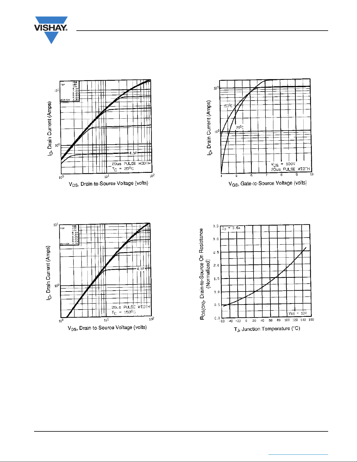
TYPICAL CHARACTERISTICS (25 °C, unless otherwise noted)
Vishay Siliconix
Fig. 1 - Typical Output Characteristics
Fig. 2 - Typical Output Characteristics
Fig. 3 - Typical Transfer Characteristics
Fig. 4 - Normalized On-Resistance vs. Temperature
Document Number: 91111 www.vishay.com
S11-1053-Rev. C, 30-May-11 3
THE PRODUCTS DESCRIBED HEREIN AND THIS DOCUMENT ARE SUBJECT TO SPECIFIC DISCLAIMERS, SET FORTH AT
This document is subject to change without notice.
www.vishay.com/doc?91000
Page 4
IRFBC30S, SiHFBC30S, IRFBC30L, SiHFBC30L
Vishay Siliconix
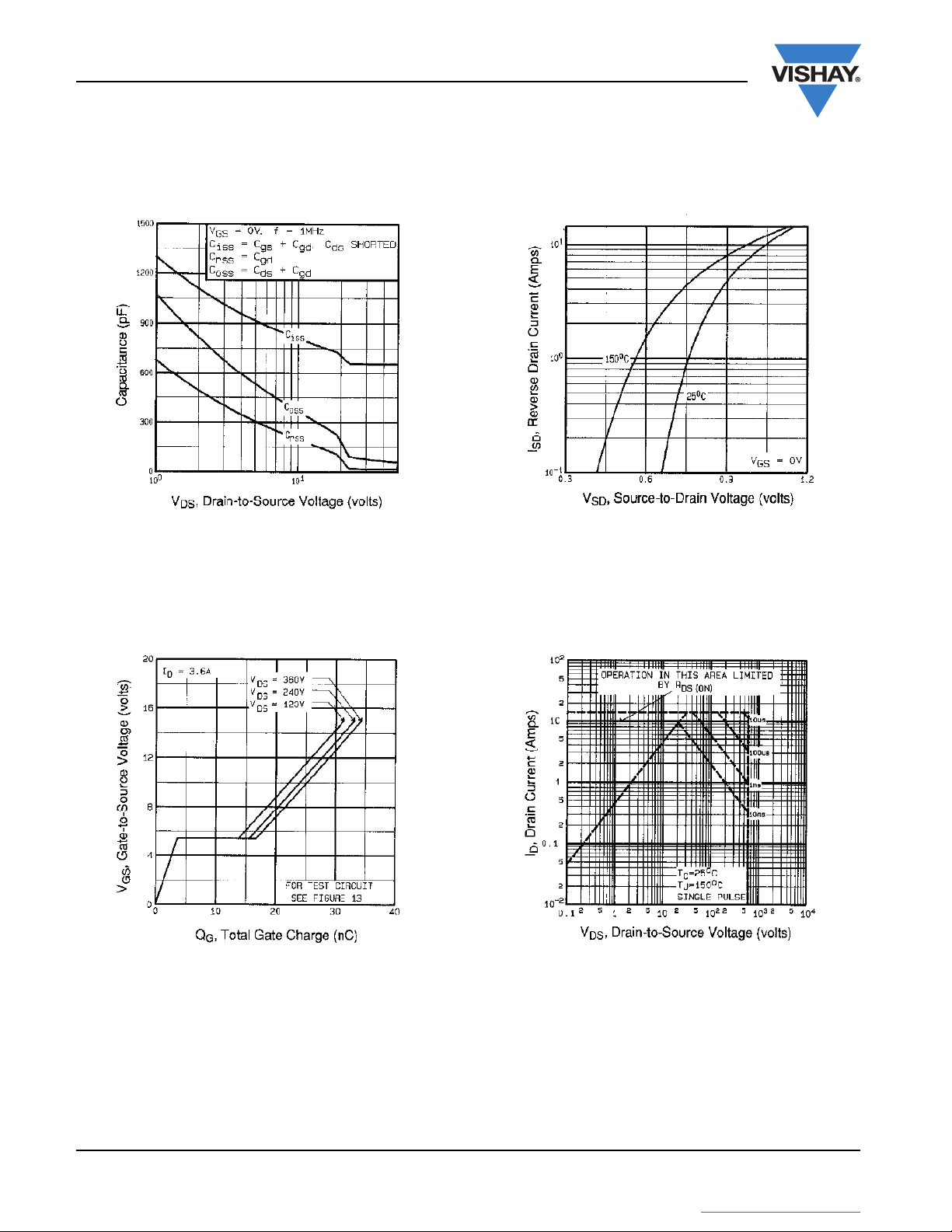
Fig. 5 - Typical Capacitance vs. Drain-to-Source Voltage
Fig. 6 - Typical Gate Charge vs. Gate-to-Source Voltage
Fig. 7 - Typical Source-Drain Diode Forward Voltage
Fig. 8 - Maximum Safe Operating Area
www.vishay.com Document Number: 91111
4 S11-1053-Rev. C, 30-May-11
THE PRODUCTS DESCRIBED HEREIN AND THIS DOCUMENT ARE SUBJECT TO SPECIFIC DISCLAIMERS, SET FORTH AT
This document is subject to change without notice.
www.vishay.com/doc?91000
Page 5

V
DS
90 %
10 %
V
GS
t
d(on)
t
r
t
d(off)
t
f
R
g
I
AS
0.01 Ω
t
p
D.U.T.
L
V
DS
+
-
V
DD
10 V
Var y t
p
to obtain
required I
AS
I
AS
V
DS
V
DD
V
DS
t
p
IRFBC30S, SiHFBC30S, IRFBC30L, SiHFBC30L
Vishay Siliconix
R
D.U.T.
D
+
V
-
DD
V
DS
V
GS
R
g
10 V
Pulse width ≤ 1 µs
Duty factor ≤ 0.1 %
Fig. 10a - Switching Time Test Circuit
Fig. 9 - Maximum Drain Current vs. Case Temperature
Fig. 11 - Maximum Effective Transient Thermal Impedance, Junction-to-Case
Fig. 10b - Switching Time Waveforms
Document Number: 91111 www.vishay.com
S11-1053-Rev. C, 30-May-11 5
THE PRODUCTS DESCRIBED HEREIN AND THIS DOCUMENT ARE SUBJECT TO SPECIFIC DISCLAIMERS, SET FORTH AT
Fig. 12a - Unclamped Inductive Test Circuit
Fig. 12b - Unclamped Inductive Waveforms
This document is subject to change without notice.
www.vishay.com/doc?91000
Page 6

D.U.T.
3 mA
V
GS
V
DS
I
G
I
D
0.3 µF
0.2 µF
50 kΩ
12 V
Current regulator
Current sampling resistors
Same type as D.U.T.
+
-
IRFBC30S, SiHFBC30S, IRFBC30L, SiHFBC30L
Vishay Siliconix
Fig. 12c - Maximum Avalanche Energy vs. Drain Current
Q
10 V
V
Q
GS
G
G
Q
GD
Charge
Fig. 13a - Maximum Avalanche Energy vs. Drain Current Fig. 13b - Gate Charge Test Circuit
www.vishay.com Document Number: 91111
6 S11-1053-Rev. C, 30-May-11
This document is subject to change without notice.
THE PRODUCTS DESCRIBED HEREIN AND THIS DOCUMENT ARE SUBJECT TO SPECIFIC DISCLAIMERS, SET FORTH AT
www.vishay.com/doc?91000
Page 7

IRFBC30S, SiHFBC30S, IRFBC30L, SiHFBC30L
Vishay Siliconix
Peak Diode Recovery dV/dt Test Circuit
D.U.T.
+
-
R
g
Driver gate drive
P.W.
+
-
Period
Circuit layout considerations
• Low stray inductance
• Ground plane
• Low leakage inductance
current transformer
• dV/dt controlled by R
• Driver same type as D.U.T.
I
controlled by duty factor “D”
•
SD
• D.U.T. - device under test
-
D =
g
Period
P.W.
+
+
V
DD
-
= 10 Va
V
GS
D.U.T. l
Reverse
recovery
current
D.U.T. V
Re-applied
voltage
Inductor current
Note
a. V
waveform
SD
Body diode forward
waveform
DS
Body diode forward drop
Ripple ≤ 5 %
= 5 V for logic level devices
GS
current
dI/dt
Diode recovery
dV/dt
V
DD
I
SD
Fig. 14 - For N-Channel
Vishay Siliconix maintains worldwide manufacturing capability. Products may be manufactured at one of several qualified locations. Reliability data for Silicon
Technology and Package Reliability represent a composite of all qualified locations. For related documents such as package/tape drawings, part marking, and
reliability data, see www.vishay.com/ppg?91111
.
Document Number: 91111 www.vishay.com
S11-1053-Rev. C, 30-May-11 7
This document is subject to change without notice.
THE PRODUCTS DESCRIBED HEREIN AND THIS DOCUMENT ARE SUBJECT TO SPECIFIC DISCLAIMERS, SET FORTH AT
www.vishay.com/doc?91000
Page 8

TO-263AB (HIGH VOLTAGE)
(Datum A)
34
E
L1
4
D
L2
4
C
1
B
B
C
3
2
B
B
Package Information
Vishay Siliconix
A
A
5
H
Detail A
B
A
c2
Gauge
plane
0° to 8°
L
L3
L4
Detail “A”
Rotated 90° CW
scale 8:1
H
B
Seating plane
A1
2 x e
Lead tip
2 x b2
2 x b
0.010 A B
MM
Plating
(c)
Section B - B and C - C
c
± 0.004 B
5
b1, b3
(b, b2)
Scale: none
M
Base
metal
c1
A
E
D1
4
5
E1
View A - A
4
MILLIMETERS INCHES MILLIMETERS INCHES
DIM. MIN. MAX. MIN. MAX. DIM. MIN. MAX. MIN. MAX.
A 4.06 4.83 0.160 0.190 D1 6.86 - 0.270 -
A1 0.00 0.25 0.000 0.010 E 9.65 10.67 0.380 0.420
b 0.51 0.99 0.020 0.039 E1 6.22 - 0.245 -
b1 0.51 0.89 0.020 0.035 e 2.54 BSC 0.100 BSC
b2 1.14 1.78 0.045 0.070 H 14.61 15.88 0.575 0.625
b3 1.14 1.73 0.045 0.068 L 1.78 2.79 0.070 0.110
c 0.38 0.74 0.015 0.029 L1 - 1.65 - 0.066
c1 0.38 0.58 0.015 0.023 L2 - 1.78 - 0.070
c2 1.14 1.65 0.045 0.065 L3 0.25 BSC 0.010 BSC
D 8.38 9.65 0.330 0.380 L4 4.78 5.28 0.188 0.208
ECN: S-82110-Rev. A, 15-Sep-08
DWG: 5970
Notes
1. Dimensioning and tolerancing per ASME Y14.5M-1994.
2. Dimensions are shown in millimeters (inches).
3. Dimension D and E do not include mold flash. Mold flash shall not exceed 0.127 mm (0.005") per side. These dimensions are measured at the
outmost extremes of the plastic body at datum A.
4. Thermal PAD contour optional within dimension E, L1, D1 and E1.
5. Dimension b1 and c1 apply to base metal only.
6. Datum A and B to be determined at datum plane H.
7. Outline conforms to JEDEC outline to TO-263AB.
Document Number: 91364 www.vishay.com
Revision: 15-Sep-08 1
Page 9

I2PAK (TO-262) (HIGH VOLTAGE)
(Datum A)
E
L1
Package Information
Vishay Siliconix
A
A
B
c2
A
E
D
L2
0.010 A B
Lead tip
B
2 x e
M
Seating
plane
C
C
B
M
3 x b2
3 x b
L
A1
A
E1
Section A - A
Plating
c
b1, b3
(b, b2)
Section B - B and C - C
Scale: None
c
D1
Base
metal
c1
MILLIMETERS INCHES MILLIMETERS INCHES
DIM. MIN. MAX. MIN. MAX. DIM. MIN. MAX. MIN. MAX.
A 4.06 4.83 0.160 0.190 D 8.38 9.65 0.330 0.380
A1 2.03 3.02 0.080 0.119 D1 6.86 - 0.270 -
b 0.51 0.99 0.020 0.039 E 9.65 10.67 0.380 0.420
b1 0.51 0.89 0.020 0.035 E1 6.22 - 0.245 -
b2 1.14 1.78 0.045 0.070 e 2.54 BSC 0.100 BSC
b3 1.14 1.73 0.045 0.068 L 13.46 14.10 0.530 0.555
c 0.38 0.74 0.015 0.029 L1 - 1.65 - 0.065
c1 0.38 0.58 0.015 0.023 L2 3.56 3.71 0.140 0.146
c2 1.14 1.65 0.045 0.065
ECN: S-82442-Rev. A, 27-Oct-08
DWG: 5977
Notes
1. Dimensioning and tolerancing per ASME Y14.5M-1994.
2. Dimension D and E do not include mold flash. Mold flash shall not exceed 0.127 mm per side. These dimensions are measured at the outmost
extremes of the plastic body.
3. Thermal pad contour optional within dimension E, L1, D1, and E1.
4. Dimension b1 and c1 apply to base metal only.
Document Number: 91367 www.vishay.com
Revision: 27-Oct-08 1
Page 10

RECOMMENDED MINIMUM PADS FOR D2PAK: 3-Lead
0.420
(10.668)
0.635
(16.129)
0.355
AN826
Vishay Siliconix
(9.017)
Return to Index
0.135
(3.429)
0.200
(5.080)
Recommended Minimum Pads
Dimensions in Inches/(mm)
0.050
(1.257)
0.145
(3.683)
Document Number: 73397
11-Apr-05
www.vishay.com
1
Page 11

Legal Disclaimer Notice
www.vishay.com
Vishay
Disclaimer
ALL PRODUCT, PRODUCT SPECIFICATIONS AND DATA ARE SUBJECT TO CHANGE WITHOUT NOTICE TO IMPROVE
RELIABILITY, FUNCTION OR DESIGN OR OTHERWISE.
Vishay Intertechnology, Inc., its affiliates, agents, and employees, and all persons acting on its or their behalf (collectively,
“Vishay”), disclaim any and all liability for any errors, inaccuracies or incompleteness contained in any datasheet or in any other
disclosure relating to any product.
Vishay makes no warranty, representation or guarantee regarding the suitability of the products for any particular purpose or
the continuing production of any product. To the maximum extent permitted by applicable law, Vishay disclaims (i) any and all
liability arising out of the application or use of any product, (ii) any and all liability, including without limitation special,
consequential or incidental damages, and (iii) any and all implied warranties, including warranties of fitness for particular
purpose, non-infringement and merchantability.
Statements regarding the suitability of products for certain types of applications are based on Vishay’s knowledge of
typical requirements that are often placed on Vishay products in generic applications. Such statements are not binding
statements about the suitability of products for a particular application. It is the customer’s responsibility to validate that a
particular product with the properties described in the product specification is suitable for use in a particular application.
Parameters provided in datasheets and / or specifications may vary in different applications and performance may vary over
time. All operating parameters, including typical parameters, must be validated for each customer application by the customer’s
technical experts. Product specifications do not expand or otherwise modify Vishay’s terms and conditions of purchase,
including but not limited to the warranty expressed therein.
Except as expressly indicated in writing, Vishay products are not designed for use in medical, life-saving, or life-sustaining
applications or for any other application in which the failure of the Vishay product could result in personal injury or death.
Customers using or selling Vishay products not expressly indicated for use in such applications do so at their own risk.
Please contact authorized Vishay personnel to obtain written terms and conditions regarding products designed for
such applications.
No license, express or implied, by estoppel or otherwise, to any intellectual property rights is granted by this document
or by any conduct of Vishay. Product names and markings noted herein may be trademarks of their respective owners.
Revision: 13-Jun-16
1
Document Number: 91000
 Loading...