

Page 1
SMPS MOSFET
S
D
G
Trr
Absolute Ma ximu m R atings
Continuous Drain Current, V
@ 10V
= 100°C
Continuous Drain Current, V
@ 10V
Pulsed Drain Current
c
Peak Diode Recovery dv/dt
e
11
V/ns
Diode Characteristics
Units
c
f
TJ = 125°C, di/dt = 100A/µs
f
f
TJ = 125°C, di/dt = 100A/µs
f
I
)
PD - 94631A
IRFB16N60L
Applications
HEXFET® Power MOSFET
• Zero Voltage Switching SMPS
V
• Telecom and Server Power Supplies
• Uninterruptible Power Supplies
DSSRDS(on)
600V
385m
• Motor Control applications
Features and Benefits
• SuperFast body diode eliminates the need for external
diodes in ZVS applications.
• Lower Gate charge results in simpler drive requirements.
• Enhanced dv/dt capabilities offer improved ruggedness.
• Higher Gate voltage threshold offers improved noise immunity
Parameter Max. Units
ID @ TC = 25°C
I
@ T
D
C
I
DM
P
@TC = 25°C
D
V
GS
dv/dt
T
J
T
STG
GS
GS
Power Dissipation 310 W
Linear Derating Factor 2.5 W/°C
Gat e-to-So urc e Voltage ±30 V
Operating Junction and -55 to + 150
Storage Temperature Range °C
Soldering Temperature, for 10 seconds 300 (1.6mm from case )
Mounting torque, 6-32 or M3 screw 1.1(10) N•m (lbf•in)
16
10 A
60
typ.
typ.
Ω 130ns 16A
.
TO-220AB
I
D
Symbol Parameter M in. Typ. Max.
I
S
I
SM
V
SD
t
rr
Q
rr
RRM
t
on
www.irf.com 1
Co nd itio ns
Continuous Source Current ––– ––– 16 MOSFET symbol
(Body Diode) A showing the
Pu lsed Sourc e C urrent ––– ––– 60 in te g ra l re v e rs e
(Body Diode)
Diode Forward Voltage ––– ––– 1.5 V
Reverse Recovery Time ––– 130 200 ns
Reverse Recovery Charge ––– 450 670 nC
Reverse Recovery Current ––– 5.8 8.7 A
Forward Turn-On Time Intrinsic turn-on time is negligible (turn-on is dominated by LS+LD
––– 240 360
––– 1080 1620
p-n junction diode.
= 25°C, IS = 16A, VGS = 0V
T
J
= 25°C, IF = 16A
T
J
= 25°C, IS = 16A, VGS = 0V
T
J
= 25°C
T
J
10/19/04
Page 2
IRFB16N60L
V
V
/∆T
R
V
I
I
R
Q
Q
Q
t
t
t
t
C
C
C
C
eff.
C
eff. (ER)
EASSingl e Puls e Avalanche En ergy.
d
IARAvalanche Current
c
EARRepe titive Ava lanche Energy
c
R
Junction-to-Case
h
R
Junction-to-Ambient
h
Static @ TJ = 25°C (unless otherw ise specified)
Symbol Parameter Min. Typ. Max. Units
(BR)DSS
∆
DS(on)
GS(th)
DSS
GSS
G
(BR)DSS
Drain-to-Source Breakdown V oltage 600 ––– ––– V
Breakdo w n Voltage Temp. Coef ficient ––– 0.3 9 ––– V/°C
J
Static Dr ain-to-Source On-Resi stance ––– 3 85 460
Gate Threshold Voltage 3.0 ––– 5.0 V
Drain-to- Source Leakage Current ––– ––– 50 µA
––– ––– 2.0 mA
Gate-to-Sourc e Forward Leakage ––– ––– 100 nA
Gate-to-Source Reverse Leakage ––– – –– -100
Internal Gate Resistance ––– 0.79 –––
VGS = 0V, ID = 250µA
Re ferenc e to 25°C , I
V
Ω
m
GS
V
DS
V
DS
V
DS
V
GS
V
GS
Ω
f = 1MHz, open drain
Dynamic @ TJ = 25°C (unless otherw ise specified)
Symbol Parameter Min. Typ. Max. Units
gfs Forwa rd Tr a nsconductance 8.3 ––– ––– S
g
gs
gd
d(on)
r
d(off)
f
iss
oss
rss
oss
oss
Total Gate Charge ––– ––– 100
Gate-to-Source Charge ––– ––– 30 nC
Gate-to-Drain ("Miller") Charge ––– ––– 46
Turn-On Delay Time ––– 20 –––
Rise Time ––– 44 ––– ns
Turn-Off Delay Time ––– 28 –––
Fall Time ––– 5.5 –––
Input Capacitance ––– 2720 –––
Output Capacitance ––– 260 –––
Rever se Transfer C apacitanc e ––– 20 ––– pF
Effective Output Capaci t ance ––– 120 –––
Effective Output Capacitance ––– 100 –––
(Energy Related)
VDS = 50V, ID = 9.0A
= 16A
I
D
V
DS
V
GS
VDD = 300V
ID = 16A
R
G
V
GS
VGS = 0V
V
DS
ƒ = 1.0MHz, See F i g. 5
V
GS
Avalanche Characteristics
Symbol Parameter Typ. Units
––– mJ
––– A
––– mJ
Thermal Resistan ce
Symbol Parameter Typ. Units
JC
θ
JA
θ
––– °C/W
––– 62
Conditions
= 1mA
D
= 10V, ID = 9.0A
f
= VGS, ID = 250µA
= 600V, VGS = 0V
= 480V, VGS = 0V, TJ = 125°C
= 30V
= -30V
Conditions
= 480V
= 10V, See Fig . 7 & 15
Ω
= 1.8
= 10V, See Fig . 11a & 11b
= 25V
= 0V,VDS = 0V to 480V
Max.
310
16
31
Max.
0.4
f
f
g
Notes:
Repetitive rating; pulse width limited by
max. junction temperature. (See Fig. 12)
Starting T
I
AS
I
SD
TJ ≤ 150°C.
2 www.irf.com
= 25°C, L = 2.5mH, RG = 25Ω,
J
= 16A.(See Figure 14a)
≤ 16A, di/dt ≤ 650A/µs, V
DD
≤ V
(BR)DSS
Pulse width ≤ 300µs; duty cycle ≤ 2%.
C
eff. is a fixed capacitance that gives the same charging time
oss
as C
while VDS is rising from 0 to 80% V
oss
C
eff.(ER) is a fixed capacitance that stores the same energy
oss
as C
while VDS is rising from 0 to 80% V
,
oss
R
is measured at TJ approximately 90°C
θ
DSS
DSS
.
.
Page 3
IRFB16N60L
1000
TOP 15V
100
)
A
(
t
n
e
r
10
r
u
C
e
c
r
u
o
S
-
o
t
-
n
i
a
r
D
,
D
I
BOTTOM 5.0V
1
0.1
0.01
VGS
12V
10V
9.0V
8.0V
7.0V
6.0V
5.0V
20µs PULSE WIDTH
Tj = 25°C
0.001
0.1 1 10 100
VDS, Drain-to-Source Voltage (V)
1000
)
Α
100
(
t
n
e
r
r
u
C
10
e
c
r
u
o
S
-
1
o
t
-
n
i
a
r
D
,
0.1
D
I
TJ = 25°C
TJ = 150°C
V
= 50V
DS
20µs PULSE WIDTH
0.01
4 6 8 10 12 14 16
VGS, Gate-to-Source Voltage ( V)
100
TOP 15V
)
A
(
t
10
n
e
r
r
u
C
e
c
r
u
o
S
-
o
t
-
n
i
a
r
D
,
D
I
BOTTOM 5.0V
1
0.1
VGS
12V
10V
9.0V
8.0V
7.0V
6.0V
5.0V
20µs PULSE WIDTH
Tj = 150°C
0.01
0.1 1 10 100
VDS, Drain-to-Source Voltage (V)
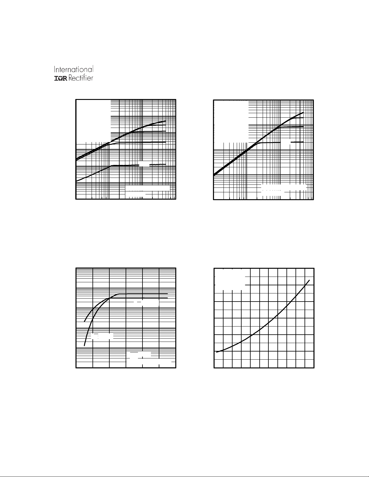
Fig 2. Typical Output CharacteristicsFig 1. Typical Output Characteristics
3.0
e
c
n
a
t
s
i
s
e
R
n
O
e
c
r
u
o
S
-
o
t
-
n
i
a
r
D
,
)
n
o
(
S
D
R
ID = 15A
V
= 10V
GS
2.5
2.0
)
d
e
z
i
1.5
l
a
m
r
o
N
(
1.0
0.5
0.0
-60 -40 -20 0 20 40 60 80 100 120 140 160
TJ , Junction Temperature (°C)
Fig 3. Typical Transfer Characteristics
Fig 4. Normalized On-Resistance
vs. Temperature
www.irf.com 3
Page 4

IRFB16N60L
100000
10000
)
F
p
(
e
1000
c
n
a
t
i
c
a
p
100
a
C
,
C
10
1
V
= 0V, f = 1 MHZ
GS
C
= C
iss
rss
oss
= C
= C
gs
gd
ds
C
C
C
rss
C
C
1 10 100 1000
VDS, Drain-to-Source Voltage (V)
Fig 5. Typical Capacitance vs.
Drain-to-Source Voltage
12.0
ID= 15A
)
10.0
V
(
e
g
a
t
l
8.0
o
V
e
c
r
u
6.0
o
S
-
o
t
-
e
t
4.0
a
G
,
S
G
2.0
V
0.0
0 10203040506070
Q
VDS= 480V
VDS= 300V
VDS= 120V
Total G ate Charge (nC)
G
+ Cgd, C
+ C
gd
iss
oss
SHORTED
ds
)
J
µ
(
y
g
r
e
n
E
100.00
)
A
(
t
n
e
r
10.00
r
u
C
n
i
a
r
D
e
s
r
e
v
1.00
e
R
,
D
S
I
0.10
25
20
15
10
5
0
0 100 200 300 400 500 600 700
V
Drain-to-Source Voltage (V)
DS,
Fig 6. Typ. Output Capacitance
Stored Energy vs. V
TJ = 150°C
TJ = 25°C
0.2 0.4 0.6 0.8 1.0 1.2 1.4 1.6
VSD, Source-to-Drain Voltage (V)
DS
V
GS
= 0V
Fig 7. Typical Gate Charge vs.
Gate-to-Source Voltage
Fig 8. Typical Source-Drain Diode
Forward Voltage
4 www.irf.com
Page 5

IRFB16N60L
+
-
V
9
1
V
1000
OPERATION IN THIS AREA
)
A
(
t
n
e
r
r
u
C
e
c
r
u
o
S
-
o
t
-
n
i
a
r
D
,
I
100
10
1
D
Tc = 25°C
Tj = 150°C
Single Pulse
LIMITED BY RDS(on)
100µsec
1msec
10msec
0.1
1 10 100 1000 10000
VDS, Drain-to-Source Voltage (V)
Fig 9. Maximum Safe Operating Area
18
16
14
)
A
(
12
t
n
e
r
r
10
u
C
n
i
8
a
r
D
6
,
D
I
4
2
0
25 50 75 100 125 150
TC , Case Temper ature (°C)
Fig 10. Maximum Drain Current vs.
Case Temperature
R
D.U.T.
D
V
DD
DS
0%
0%
GS
t
d(on)tr
t
d(off)tf
Fig 11b. Switching Time Waveforms
V
DS
V
GS
R
G
10V
Pulse Width ≤ 1 µs
Duty Factor ≤ 0.1 %
Fig 11a. Switching Time Test Circuit
www.irf.com 5
Page 6

IRFB16N60L
1
)
C
J
h
t
Z
(
e
s
n
o
p
s
e
R
l
a
m
r
e
h
T
0.001
0.1
0.01
D = 0.50
0.20
0.10
0.05
0.02
0.01
SINGLE PULSE
( THERMAL RESPONSE )
1E-006 1E-005 0.0001 0.001 0.01 0.1 1
Notes:
1. Duty factor D = t / t
2. Peak T = P x Z + T
J DM thJC C
1 2
P
DM
t
t1 , Rectangular Pulse Duration (sec)
Fig 12. Maximum Effective Transient Thermal Impedance, Junction-to-Case
1
t
2
5.0
)
V
(
4.5
e
g
a
t
l
o
4.0
V
d
l
o
h
s
3.5
e
r
h
t
e
t
a
3.0
G
)
h
t
(
S
2.5
G
V
2.0
-75 -50 -25 0 25 50 75 100 125 150 175
ID = 250µA
TJ , Temperature ( °C )
Fig 13. Threshold Voltage vs. Temperature
6 www.irf.com
Page 7

IRFB16N60L
S
Current Regulator
I
A
V
600
)
J
m
(
y
500
g
r
e
n
E
e
400
h
c
n
a
l
a
v
300
A
e
s
l
u
P
200
e
l
g
n
i
S
100
,
S
A
E
0
25 50 75 100 125 150
TOP 7.2A
BOTTOM16A
Starting TJ , Junction Temperature (°C)
Fig 14a. Maximum Avalanche Energy
vs. Drain Current
15V
V
DS
L
DRIVER
I
D
10A
t
V
(BR)DSS
p
R
G
20V
Fig 14b. Unclamped Inductive Test Circuit
12V
V
GS
Fig 15a. Gate Charge Test Circuit
D.U.T
I
AS
0.01
t
p
Same Type as D.U.T.
.2µF
Ω
50KΩ
.3µF
3mA
Current Sampling Resistors
+
V
DD
-
AS
Fig 14c. Unclamped Inductive Waveforms
Q
G
VGS V
Q
GS
D.U.T.
+
V
D
-
G
I
I
G
D
Q
GD
Charge
Fig 15b. Basic Gate Charge Waveform
www.irf.com 7
Page 8

IRFB16N60L
R
V
+
-
Peak Diode Recovery dv/dt Test Circuit
+
D.U.T
-
R
G
Driver Gate Drive
P.W.
+
Circuit Layout Considerations
• Low Stray Inductance
• Ground Plane
• Low Leakage Inductance
Current Transformer
-
-
• dv/dt controlled by R
• Driver same type as D.U.T.
G
• ISD controlled by Duty Factor "D"
• D.U.T. - Device Under Test
Period
D =
P.W.
Period
+
V
DD
VGS=10V
*
D.U.T. ISDWaveform
Reverse
Recovery
Current
e-Applied
oltage
D.U.T. VDSWaveform
Inductor Curent
* V
= 5V for Logic Level Devices
GS
Body Diode Forward
Current
di/dt
Diode Recovery
dv/dt
Body Diode Forward Drop
Ripple ≤ 5%
V
DD
I
SD
Fig 16. For N-Channel HEXFET® Power MOSFETs
8 www.irf.com
Page 9

K
TO-220AB Package Outline
R
Dimensions are shown in millimeters (inches)
IRFB16N60L
10.54 (.415)
2.87 (.113)
2.62 (.103)
15.24 (.600)
14.84 (.584)
14.09 (.555)
13.47 (.530)
1.40 (.055)
3X
1.15 (.045)
2.54 (.100)
NOTES:
1 DIMENSIONING & TOLERANCING PER ANSI Y14.5M, 1982. 3 OUTLINE CONFORMS TO JEDEC OUTLINE TO-220AB.
2 CONTROLLING DIMENSION : INCH 4 HEATSINK & LEAD MEASUREMENTS DO NOT INCLUDE BURRS.
2X
10.29 (.405)
4
1 2 3
3.78 (.149)
3.54 (.139)
- A -
6.47 (.255)
6.10 (.240)
1.15 (.045)
MIN
4.06 (.160)
3.55 (.140)
0.93 (.037)
3X
0.69 (.027)
0.36 (.014) M B A M
4.69 (.185)
4.20 (.165)
- B -
1.32 (.052)
1.22 (.048)
2.92 (.115)
2.64 (.104)
3X
LEAD ASSIGNMENTS
LEAD ASSIGNMENTS
HEXFET
1 - GATE
2 - DRAIN
1- GATE
3 - SOURCE
2- DRAIN
3- SOURCE
4 - DRAIN
4- DRAIN
0.55 (.022)
0.46 (.018)
TO-220AB Part Marking Information
EXAMPLE:
THIS IS AN IRF1010
LOT CODE 1789
ASSEMBLED ON WW 19, 1997
IN THE ASS E MBLY LINE "C"
Note: "P" in assembly line
position indicates "Lead-Free"
INTERNATIONAL
RECTIFIER
LOGO
ASSEMBLY
LOT CODE
IGBTs, CoPAC
1- GATE
2- COLLECTOR
3- EMITTER
4- COLLECTOR
PART NUMBE
DATE CODE
YE AR 7 = 1997
WEEK 19
LINE C
TO-220AB package is not recommended for Surface Mount Application.
Data and specifications subject to change without notice.
This product has been designed and qualified for the Automotive [Q101] market.
Qualification Standards can be found on IR’s Web site.
IR WORLD HEADQUARTERS: 233 Kansas St., El Segundo, California 90245, USA Tel: (310) 252-7105
TAC Fax: (310) 252-7903
Visit us at www.irf.com for sales contact information.10/04
www.irf.com 9
 Loading...