

Page 1
www.vishay.com
S
G
D
P-Channel MOSFET
TO-220AB
G
D
S
IRF9Z30, SiHF9Z30
Vishay Siliconix
Power MOSFET
PRODUCT SUMMARY
VDS (V) - 50
R
()V
DS(on)
Q
(Max.) (nC) 39
g
Q
(nC) 10
gs
Q
(nC) 15
gd
Configuration Single
= - 10 V 0.14
GS
FEATURES
• P-Channel Versatility
• Compact Plastic Package
• Fast Switching
• Low Drive Current
• Ease of Paralleling
• Excellent Temperature Stability
• Material categorization: For definitions of compliance
please see www.vishay.com/doc?99912
Note
* Lead (Pb)-containing terminations are not RoHS-compliant.
Exemptions may apply.
DESCRIPTION
The power MOSFET technology is the key to Vishay’s
advanced line of power MOSFET transistors. The efficient
geometry and unique processing of the power MOSFET
design achieve very low on-state resistance combined with
high transconductance and extreme device ruggedness.
The p-channel power MOSFET’s are designed for
application which require the convenience of reverse
polarity operation. They retain all of the features of the more
common n-channel Power MOSFET’s such as voltage
control, very fast switching, ease of paralleling, and
excellent temperature stability.
P-channel power MOSFETs are intended for use in power
stages where complementary symmetry with n-channel
devices offers circuit simplification. They are also very useful
in drive stages because of the circuit versatility offered by
the reverse polarity connection. Applications include motor
control, audio amplifiers, switched mode converters, control
circuits and pulse amplifiers.
ORDERING INFORMATION
Package TO-220AB
Lead (Pb)-free
SnPb
IRF9Z30PbF
SiHF9Z30-E3
IRF9Z30
SiHF9Z30
ABSOLUTE MAXIMUM RATINGS (TC = 25 °C, unless otherwise noted)
PARAMETER SYMBOL LIMIT UNIT
Drain-Source Voltage V
Gate-Source Voltage V
T
= 25 °C
Continuous Drain Current V
Pulsed Drain Current
Linear Derating Factor 0.59 W/°C
Inductive Current, Clamped L = 100 μH I
Unclamped Inductive Current (Avalanche Current) I
Maximum Power Dissipation T
Operating Junction and Storage Temperature Range T
Soldering Recommendations (Peak Temperature) for 10 s 300
Notes
a. Repetitive rating; pulse width limited by maximum junction temperature (see fig. 14).
b. V
= - 25 V, starting TJ = 25 °C, L =100 μH, Rg = 25
DD
c. 0.063" (1.6 mm) from case.
S12-3048-Rev. A, 24-Dec-12
THIS DOCUMENT IS SUBJECT TO CHANGE WITHOUT NOTICE. THE PRODUCTS DESCRIBED HEREIN AND THIS DOCUMENT
a
For technical questions, contact: hvm@vishay.com
ARE SUBJECT TO SPECIFIC DISCLAIMERS, SET FORTH AT www.vishay.com/doc?91000
at - 10 V
GS
C
= 100 °C - 11
C
= 25 °C P
C
1
DS
± 20
GS
I
D
IDM - 60
LM
L
D
, T
J
stg
- 50
- 18
- 60 A
- 3.1 A
74 W
- 55 to + 150
c
Document Number: 91459
V
AT
°C
Page 2
IRF9Z30, SiHF9Z30
S
D
G
www.vishay.com
THERMAL RESISTANCE RATINGS
PARAMETER SYMBOL TYP. MAX. UNIT
Maximum Junction-to-Ambient R
Maximum Junction-to-Case (Drain) R
thJA
thJC
-80
-1.7
SPECIFICATIONS (TJ = 25 °C, unless otherwise noted)
PARAMETER SYMBOL TEST CONDITIONS MIN. TYP. MAX. UNIT
Static
Drain-Source Breakdown Voltage V
Gate-Source Threshold Voltage V
Gate-Source Leakage I
Zero Gate Voltage Drain Current I
Drain-Source On-State Resistance R
Forward Transconductance g
Dynamic
Input Capacitance C
Reverse Transfer Capacitance C
Total Gate Charge Q
Gate-Drain Charge Q
Turn-On Delay Time t
Rise Time t
Turn-Off Delay Time t
Fall Time t
Drain-Source Body Diode Characteristics
DS
GS(th)
V
GSS
DSS
VGS = - 10 V ID = - 9.3 A
DS(on)
fs
iss
- 570 -
oss
- 140 -
rss
g
-6.910
gs
-9.715
gd
d(on)
r
-2132
d(off)
-6496
f
VGS = 0 V, ID = - 250 μA - 50 - -
VDS = VGS, ID = - 250 μA - 2.0 -
= ± 20 V - - ± 500
GS
VDS = max. rating, VGS = 0 V - - - 250
= max. rating x 0.8, VGS = 0 V,
V
DS
T
=125 °C
J
VDS = 2 x VGS, IDS = - 9 A
b
b
VGS = 0 V,
V
= - 25 V,
DS
f = 1.0 MHz, see fig. 9
= - 18 A, VDS = - 0.8
I
V
= - 10 V
GS
V
R
= 13 , RD = 1.3, see fig. 16
g
(MOSFET switching times are
D
max. rating. see fig. 17
= - 25 V, ID = - 18 A,
DD
essentially independent of operating
temperature)
Vishay Siliconix
°C/W
- 4.0 V
- - - 1000
- 0.093 0.14
3.1 4.7 -
- 900 -
-2639
-1218
- 110 170
V
nA
μA
S
pFOutput Capacitance C
nC Gate-Source Charge Q
ns
Continuous Source-Drain Diode Current I
Pulsed Diode Forward Current
a
Body Diode Voltage V
Body Diode Reverse Recovery Time t
Body Diode Reverse Recovery Charge Q
S
MOSFET symbol
showing the
integral reverse
I
SM
SD
rr
rr
p - n junction diode
TJ = 25 °C, IS = - 18 A, VGS = 0 V
b
TJ = 25 °C, IF = - 18 A, dI/dt = 100 A/μs
--- 18
--- 60
--- 6.3
54 120 250
b
0.20 0.47 1.1
A
V
ns
μC
Notes
a. Repetitive rating; pulse width limited by maximum junction temperature (see fig. 14).
b. Pulse width 300 μs; duty cycle 2 %.
S12-3048-Rev. A, 24-Dec-12
THIS DOCUMENT IS SUBJECT TO CHANGE WITHOUT NOTICE. THE PRODUCTS DESCRIBED HEREIN AND THIS DOCUMENT
ARE SUBJECT TO SPECIFIC DISCLAIMERS, SET FORTH AT www.vishay.com/doc?91000
For technical questions, contact: hvm@vishay.com
2
Document Number: 91459
Page 3
www.vishay.com
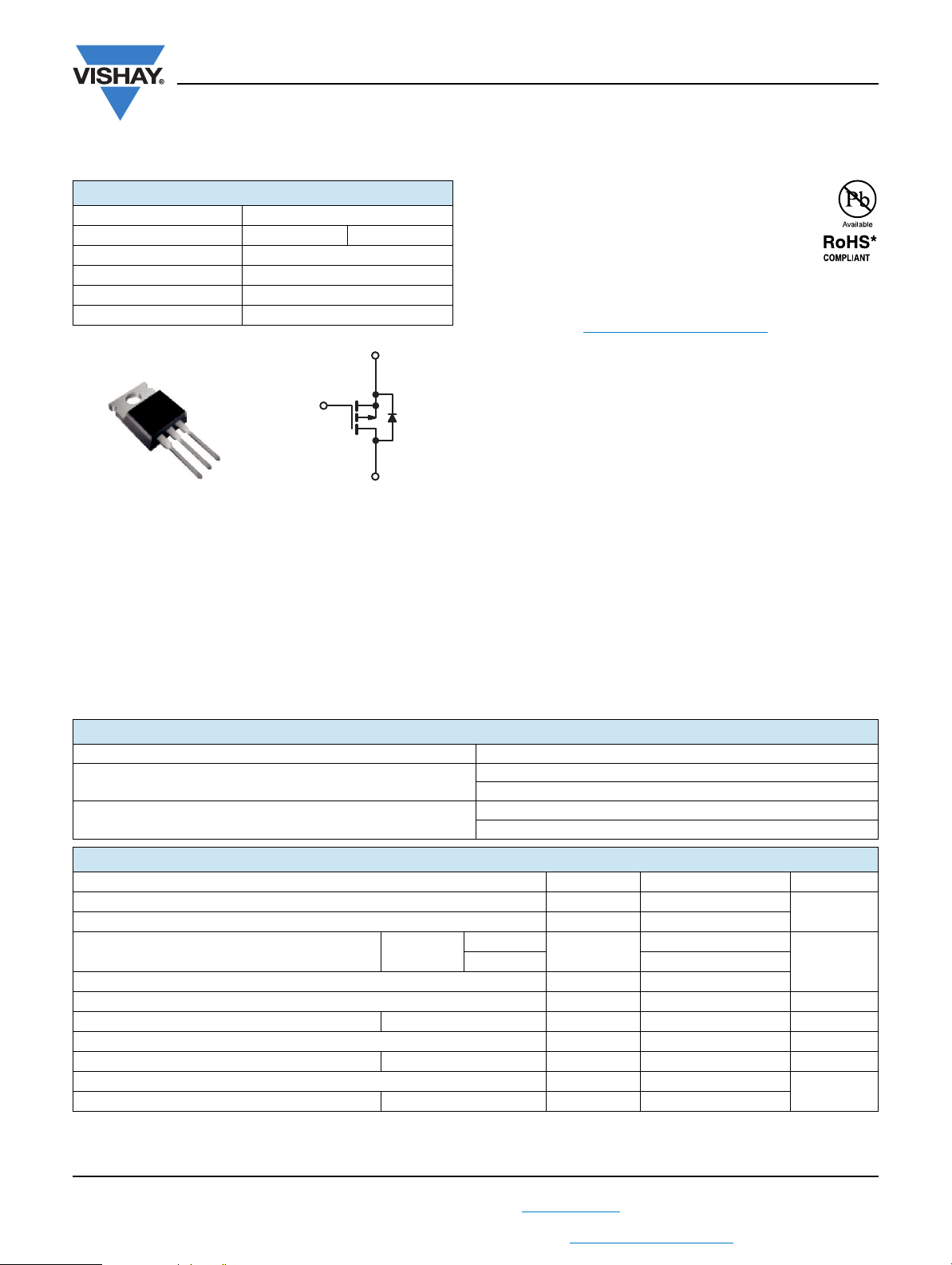
0 5 10 15 20 25
- 8 V
80 μs Pulse Test
- 7 V
VGS = - 5 V
25
20
15
10
5
0
- 4 V
- 5 V
- 10 V
- VDS, Drain-to-Source Voltage (V)
- I
D
, Drain Current (A)
10
2
10
1
0
- V
GS
,
Gate-to-Source Voltage (V)
- I
D
, Drain Current (A)
0.1
5
2
5
2
5
2
246
8
10
80 µs Pulse Test
V
DS
= 2 x V
GS
TJ = 25 °C
TJ = 150 °C
- V
DS
,
Drain-to-Source Voltage (V)
- I
D
, Drain Current (A)
- 10 V
- 8 V
- 7 V
VGS = - 5 V
- 5 V
- 4 V
80 μs Pulse Test
0
1
2
3
4
5
25
20
15
10
5
0
- VDS, Drain-to-Source Voltage (V)
- I
D
, Drain Current (A)
Operation in this Area Limited
by R
DS(on)
SiHF9Z30
SiHF9Z32
SiHF9Z30
SiHF9Z32
TC = 25 °C
T
J
= 150 °C
Single Pulse
10 μs
100 μs
1 μs
10 μs
DC
1
2
510
2
5
10
2
1
5
2
10
2
5
10
2
2
5
10
3
TYPICAL CHARACTERISTICS (25 °C, unless otherwise noted)
IRF9Z30, SiHF9Z30
Vishay Siliconix
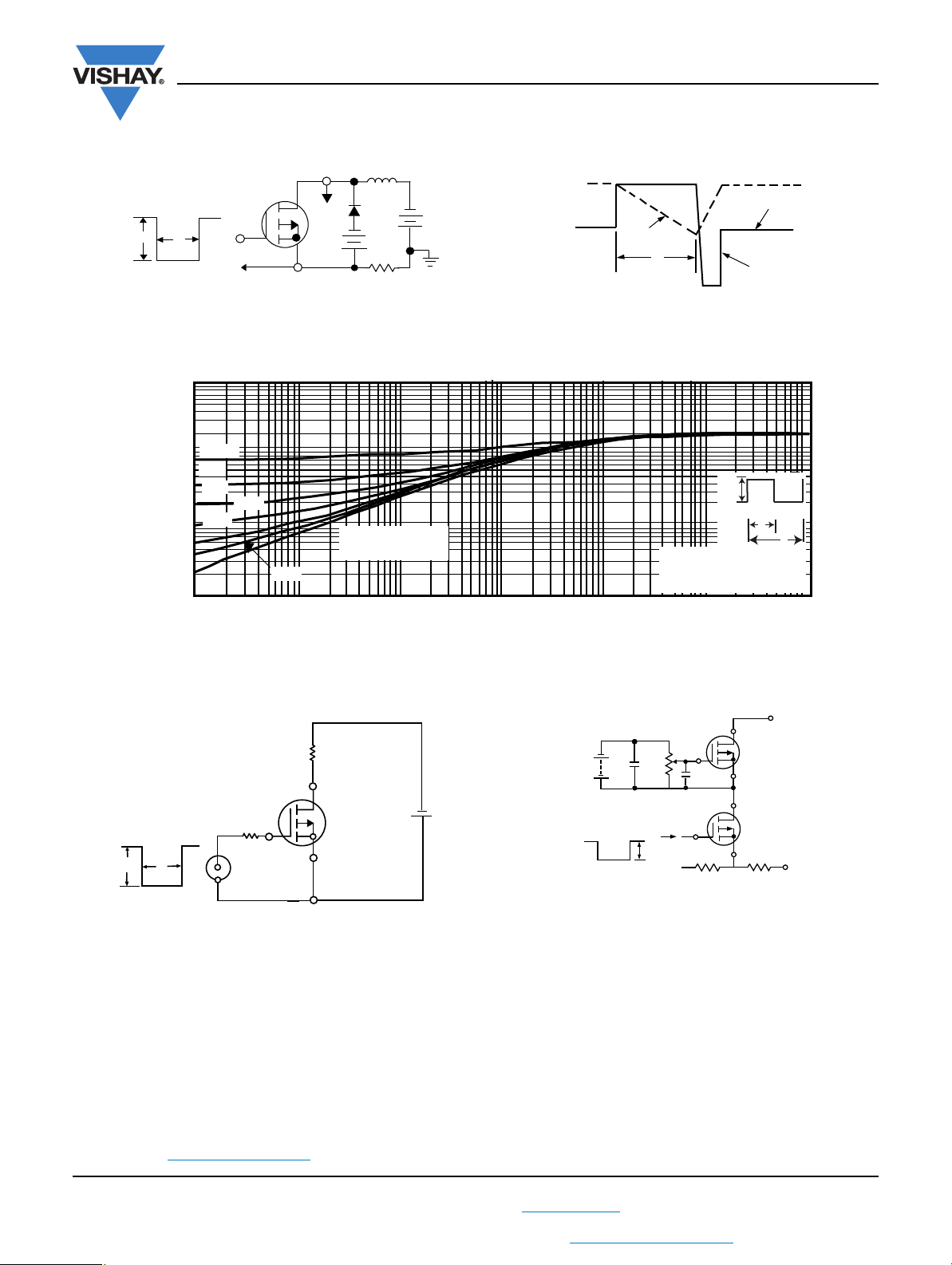
Fig. 1 - Typical Output Characteristics
Fig. 2 - Typical Transfer Characteristics
Fig. 3 - Typical Saturation Characteristics
Fig. 4 - Maximum Safe Operating Area
S12-3048-Rev. A, 24-Dec-12
THIS DOCUMENT IS SUBJECT TO CHANGE WITHOUT NOTICE. THE PRODUCTS DESCRIBED HEREIN AND THIS DOCUMENT
ARE SUBJECT TO SPECIFIC DISCLAIMERS, SET FORTH AT www.vishay.com/doc?91000
For technical questions, contact: hvm@vishay.com
3
Document Number: 91459
Page 4

www.vishay.com
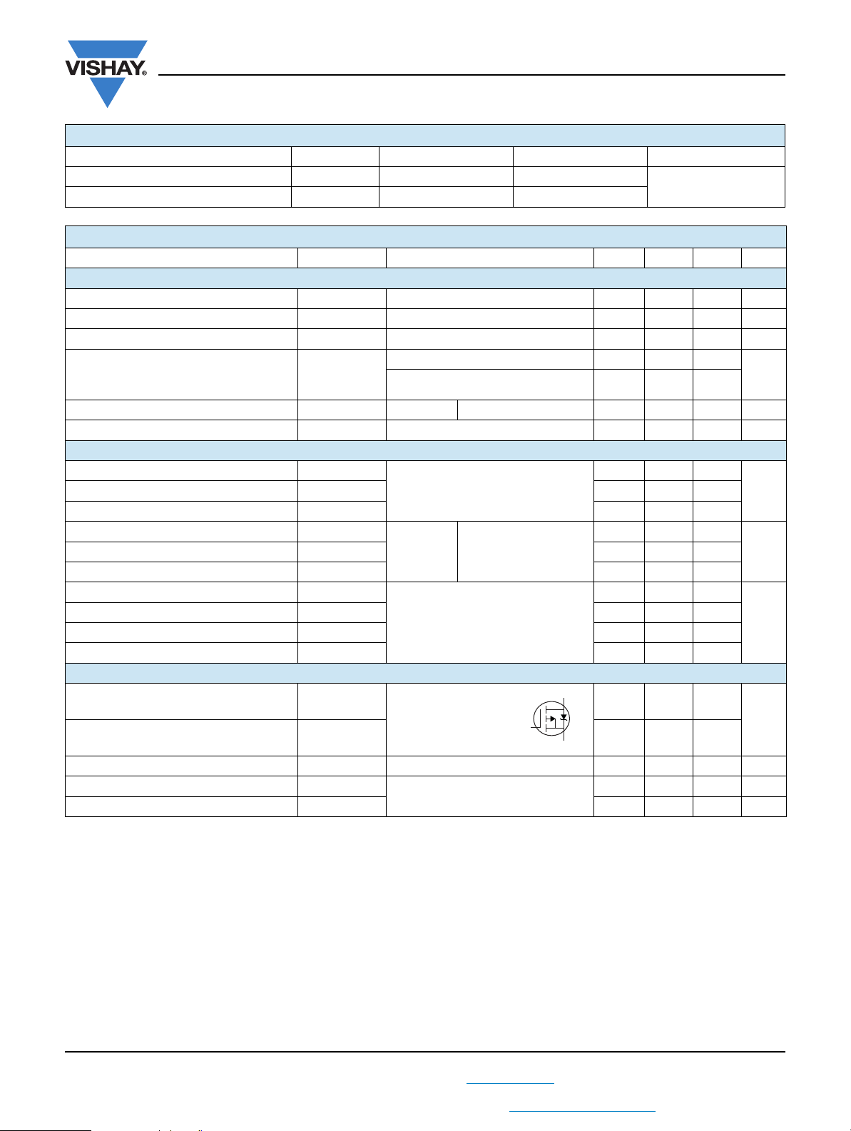
80 μs Pulse Test
V
DS
= 2 x V
GS
TJ = 25 ° C
TJ = 150 °C
04
8
12 20
10
8
6
4
2
0
15
- ID, Drain Current (A)
g
fs
, Transconductance (S)
- VSD, Source-to-Drain Voltage (V)
- I
SD
, Reverse Drain Current (A)
TJ = 25 °C
T
J
= 150 °C
0
2
4
68
10
10
2
5
2
10
5
2
1
5
2
0.1
IRF9Z30, SiHF9Z30
1.25
ID = 1 mA
1.15
1.05
0.95
Voltage (Normalized)
0.85
, Drain-to-Source Breakdown
DS
V
0.75
- 60 - 40 - 20 0 20 40 60 80 100
TJ, Junction Temperature (°C)
Vishay Siliconix
140 160
120
Fig. 5 - Typical Transconductance vs. Drain Current
Fig. 6 - Typical Source-Drain Diode Forward Voltage
Fig. 7 - Breakdown Voltage vs. Temperature
3.0
I
= - 18 A
D
= - 10 V
V
GS
2.4
1.8
1.2
(Normalized)
0.6
, Drain-to-Source On Resistance
DS(on)
0.0
R
- 60 - 40 - 20 0 20 40 60 80 100 120 140 160
TJ, Junction Temperature (°C)
Fig. 8 - Normalized On-Resistance vs. Temperature
S12-3048-Rev. A, 24-Dec-12
4
Document Number: 91459
For technical questions, contact: hvm@vishay.com
THIS DOCUMENT IS SUBJECT TO CHANGE WITHOUT NOTICE. THE PRODUCTS DESCRIBED HEREIN AND THIS DOCUMENT
ARE SUBJECT TO SPECIFIC DISCLAIMERS, SET FORTH AT www.vishay.com/doc?91000
Page 5
www.vishay.com
Capacitance (pF)
- V
DS
,
Drain-to-Source Voltage (V)
C
iss
C
oss
C
rss
1
2
5
2
10
2
10
5
0
800
1200
1600
2000
400
V
GS
= 0 V, f = 1 MHz
C
iss
= Cgs + Cgd, Cds Shorted
C
rss
= C
gd
C
oss
= Cds + C
gd
80 μ
s Pulse Test
VGS = - 10 V
VGS = - 20 V
0
12 24 36 48
60
0.4
0.8
1.2
1.6
2.0
- I
D
, Drain Current (A)
R
DS(on)
, Drain to Source on Resistance
0.0
- I
D
, Drain Current (A)
TC, Case Temperature (°C)
25 1501251007550
SiHF9Z32
SiHF9Z30
0
4
8
12
16
20
IRF9Z30, SiHF9Z30
Vishay Siliconix
Fig. 9 - Typical Capacitance vs. Drain-to-Source Voltage
20
ID = - 18 A
16
12
, Gate-to-Source Voltage (V)
GS
- V
8
4
0
020
10
VDS = - 40 V
For test circuit
see gure 17
30 40 50
Qg, Total Gate Charge (nC)
Fig. 10 - Typical Gate Charge vs. Gate-to-Source Voltage
Fig. 11 - Typical On-Resistance vs. Drain Current
Fig. 12 - Maximum Drain Current vs. Case Temperature
S12-3048-Rev. A, 24-Dec-12
5
Document Number: 91459
For technical questions, contact: hvm@vishay.com
THIS DOCUMENT IS SUBJECT TO CHANGE WITHOUT NOTICE. THE PRODUCTS DESCRIBED HEREIN AND THIS DOCUMENT
ARE SUBJECT TO SPECIFIC DISCLAIMERS, SET FORTH AT www.vishay.com/doc?91000
Page 6
www.vishay.com
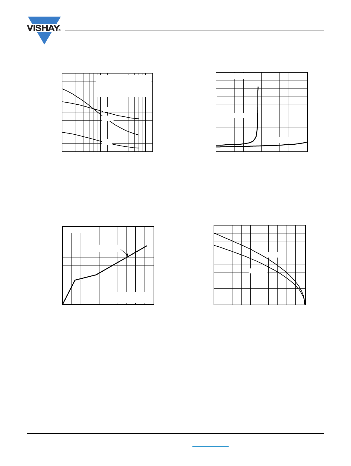
Vary tp to obtain
required peak I
L
VDD = 0 5 8 V
DS
EC = 0 75 BV
DS
-
+
V
DD
L
E
C
DUT
I
L
VGS = - 10 V
t
p
0.05 Ω
V
DSS
10
1
0.1
10
-2
10
-5
10
-4
10
-3
10
-2
0.1 1 10
t1, Rectangular Pulse Duration (s)
Thermal Response (Z
thJC
)
0 = 0.5
0.2
0.1
0.05
0.02
0.01
Single Pulse
(Thermal Response)
P
DM
t
1
t
2
Notes:
1. Duty Factor, D = t
1/t2
2. Peak Tj = PDM x Z
thJC
+ T
C
-
+
R
D
D.U.T
R
G
PS
Vary I
P
to obtain
required peak I
L
VGS = - 10 V
t
p
12 V
battery
0.2 μF
50 kΩ
0.3 μF
Current
regulator
- V
DS
(Isolated
supply)
Same type
as D.U.T
D.U.T
D
G
S
I
D
I
G
Current
sampling
resistor
Current
sampling
resistor
+ V
DS
- 1.5 mA
IRF9Z30, SiHF9Z30
Vishay Siliconix
V
DD
I
L
t
p
V
DS
Fig. 13a - Unclamped Inductive Test Circuit
Fig. 14 - Maximum Effective Transient Thermal Impedance, Junction-to-Case vs. Pulse Duration
Fig. 13b - Unclamped Inductive Load Test Waveforms
Vishay Siliconix maintains worldwide manufacturing capability. Products may be manufactured at one of several qualified locations. Reliability data for Silicon
Technology and Package Reliability represent a composite of all qualified locations. For related documents such as package/tape drawings, part marking, and
reliability data, see www.vishay.com/ppg?91459
S12-3048-Rev. A, 24-Dec-12
Fig. 15 - Switching Time Test Circuit Fig. 16 - Gate Charge Test Circuit
THIS DOCUMENT IS SUBJECT TO CHANGE WITHOUT NOTICE. THE PRODUCTS DESCRIBED HEREIN AND THIS DOCUMENT
ARE SUBJECT TO SPECIFIC DISCLAIMERS, SET FORTH AT www.vishay.com/doc?91000
.
For technical questions, contact: hvm@vishay.com
6
Document Number: 91459
Page 7
www.vishay.com
M
*
3
2
1
L
L(1)
D
H(1)
Q
Ø P
A
F
J(1)
b(1)
e(1)
e
E
b
C
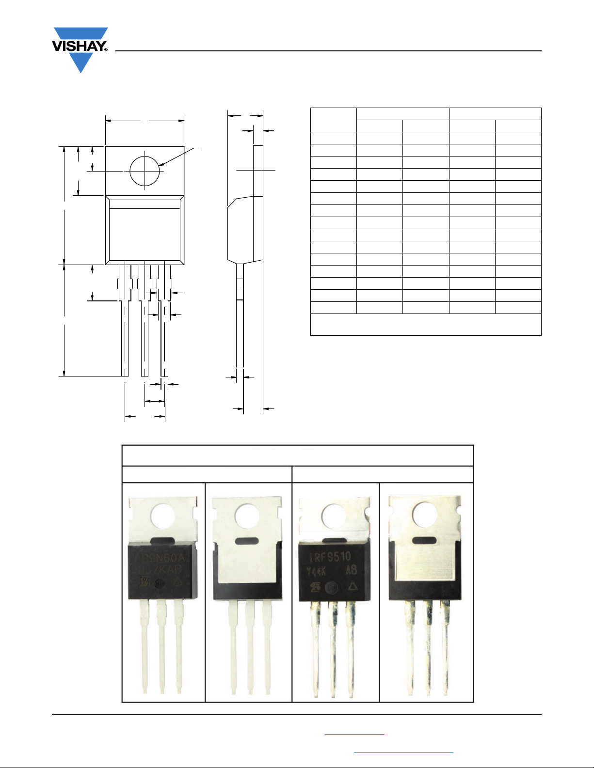
Package Information
Vishay Siliconix
TO-220-1
DIM.
A 4.24 4.65 0.167 0.183
b 0.69 1.02 0.027 0.040
b(1) 1.14 1.78 0.045 0.070
c 0.36 0.61 0.014 0.024
D 14.33 15.85 0.564 0.624
E 9.96 10.52 0.392 0.414
e 2.41 2.67 0.095 0.105
e(1) 4.88 5.28 0.192 0.208
F 1.14 1.40 0.045 0.055
H(1) 6.10 6.71 0.240 0.264
J(1) 2.41 2.92 0.095 0.115
L 13.36 14.40 0.526 0.567
L(1) 3.33 4.04 0.131 0.159
Ø P 3.53 3.94 0.139 0.155
Q 2.54 3.00 0.100 0.118
ECN: X15-0364-Rev. C, 14-Dec-15
DWG: 6031
Note
• M* = 0.052 inches to 0.064 inches (dimension including
protrusion), heatsink hole for HVM
MILLIMETERS INCHES
MIN. MAX. MIN. MAX.
ARE SUBJECT TO SPECIFIC DISCLAIMERS, SET FORTH AT www.vishay.com/doc?91000
Revison: 14-Dec-15
THIS DOCUMENT IS SUBJECT TO CHANGE WITHOUT NOTICE. THE PRODUCTS DESCRIBED HEREIN AND THIS DOCUMENT
ASE Xi’an
For technical questions, contact: hvm@vishay.com
Package Picture
1
Document Number: 66542
Page 8

Legal Disclaimer Notice
www.vishay.com
Vishay
Disclaimer
ALL PRODUCT, PRODUCT SPECIFICATIONS AND DATA ARE SUBJECT TO CHANGE WITHOUT NOTICE TO IMPROVE
RELIABILITY, FUNCTION OR DESIGN OR OTHERWISE.
Vishay Intertechnology, Inc., its affiliates, agents, and employees, and all persons acting on its or their behalf (collectively,
“Vishay”), disclaim any and all liability for any errors, inaccuracies or incompleteness contained in any datasheet or in any other
disclosure relating to any product.
Vishay makes no warranty, representation or guarantee regarding the suitability of the products for any particular purpose or
the continuing production of any product. To the maximum extent permitted by applicable law, Vishay disclaims (i) any and all
liability arising out of the application or use of any product, (ii) any and all liability, including without limitation special,
consequential or incidental damages, and (iii) any and all implied warranties, including warranties of fitness for particular
purpose, non-infringement and merchantability.
Statements regarding the suitability of products for certain types of applications are based on Vishay’s knowledge of
typical requirements that are often placed on Vishay products in generic applications. Such statements are not binding
statements about the suitability of products for a particular application. It is the customer’s responsibility to validate that a
particular product with the properties described in the product specification is suitable for use in a particular application.
Parameters provided in datasheets and / or specifications may vary in different applications and performance may vary over
time. All operating parameters, including typical parameters, must be validated for each customer application by the customer’s
technical experts. Product specifications do not expand or otherwise modify Vishay’s terms and conditions of purchase,
including but not limited to the warranty expressed therein.
Except as expressly indicated in writing, Vishay products are not designed for use in medical, life-saving, or life-sustaining
applications or for any other application in which the failure of the Vishay product could result in personal injury or death.
Customers using or selling Vishay products not expressly indicated for use in such applications do so at their own risk.
Please contact authorized Vishay personnel to obtain written terms and conditions regarding products designed for
such applications.
No license, express or implied, by estoppel or otherwise, to any intellectual property rights is granted by this document
or by any conduct of Vishay. Product names and markings noted herein may be trademarks of their respective owners.
Revision: 13-Jun-16
1
Document Number: 91000
 Loading...