

Page 1
i179012
1
2
3
4
8
7
6
5
E
C
C
E
A
C
C
A
A
C
C
A
A
C
C
A
E
C
C
E
E
C
C
E
16
15
14
13
12
11
10
9
1
2
3
4
5
6
7
8
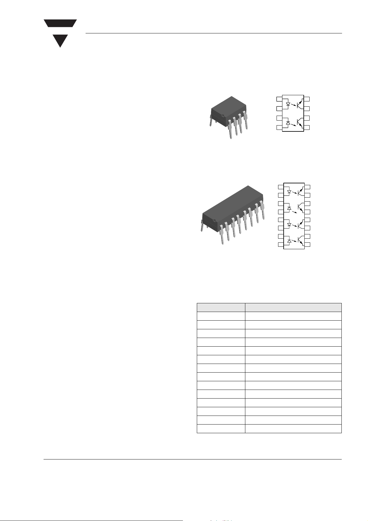
Dual Channel
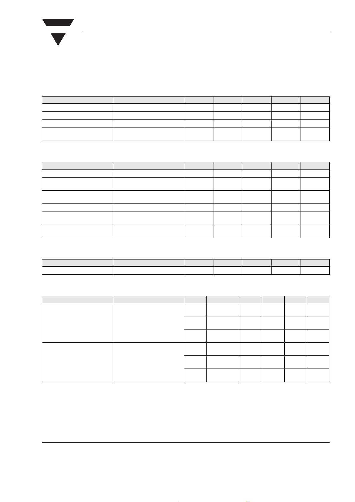
Quad Channel
VISHAY
ILD1/ 2/ 5 / ILQ1/ 2/ 5
Vishay Semiconductors
Optocoupler, Phototransistor Output (Dual, Quad Channel)
Features
• Current Transfer Ratio at IF = 10 mA
• Isolation Test Voltage, 5300 V
Agency Approvals
• UL - File No. E52744 system Code H or J
• CSA 93751
• BSI IEC60950 IEC60965
• DIN EN 60747-5-2 (VDE0884)
DIN EN 60747-5-5 pending
Available with Option 1
• FIMKO
Description
The ILD1/ 2/ 5/ ILQ1/ 2/ 5 are optically coupled isolated pairs employing GaAs infrared LEDs and silicon
NPN phototransistor. Signal information, including a
DC level, can be transmitted by the drive while maintaining a high degree of electrical isolation between
input and output. The ILD1/ 2/ 5/ ILQ1/ 2/ 5 are especially designed for driving medium-speed logic and
can be used to eliminate troublesome ground loop
and noise problems. Also these couplers can be used
to replace relays and transformers in many digital
interface applications such as CTR modulation.
The ILD1/ 2/ 5 has two isolated channels in a single
DIP package and the ILQ1/ 2/ 5 has four isolated
channels per package.
Document Number 83646
Rev. 1.3, 10-Jun-04
RMS
Order Information
Part Remarks
ILD1 CTR > 20 %, DIP-8
ILQ1 CTR > 20 %, DIP-16
ILD2 CTR > 100 %, DIP-8
ILQ2 CTR > 100 %, DIP-16
ILD5 CTR > 50 %, DIP-8
ILQ5 CTR > 50 %, DIP-16
ILD1-X007 CTR > 20 %, SMD-8 (option 7)
ILD1-X009 CTR > 20 %, SMD-8 (option 9)
ILD2-X006 CTR > 100 %, DIP-8 400 mil (option 6)
ILD2-X007 CTR > 100 %, SMD-8 (option 7)
ILD2-X009 CTR > 100 %, SMD-8 (option 9)
ILD5-X009 CTR > 50 %, SMD-8 (option 9)
ILQ1-X009 CTR > 20 %, SMD-16 (option 9)
ILQ2-X009 CTR > 100 %, SMD-16 (option 9)
For additional information on the available options refer to
Option Information.
www.vishay.com
1
Page 2

ILD1/ 2/ 5 / ILQ1/ 2/ 5
VISHAY
Vishay Semiconductors
Absolute Maximum Ratings
T
= 25 °C, unless otherwise specified
amb
Stresses in excess of the absolute Maximum Ratings can cause permanent damage to the device. Functional operation of the device is
not implied at these or any other conditions in excess of those given in the operational sections of this document. Exposure to absolute
Maximum Rating for extended periods of the time can adversely affect reliability.
Input
Parameter Test condition Symbol Val ue Unit
Reverse voltage V
Forward current I
Surge current I
Power dissipation P
R
F
FSM
diss
6.0 V
60 mA
2.5 A
100 mW
Derate linearly from 25 °C 1.3 mW/°C
Output
Paramet er Test condition Part Symbol Val ue Unit
Collector-emitter reverse voltage ILD1 V
ILQ1 V
ILD2 V
ILQ2 V
ILD5 V
ILQ5 V
Collector current I
t < 1.0 ms I
Power dissipation P
CER
CER
CER
CER
CER
CER
C
C
diss
Derate linearly from 25 °C 2.6 mW/°C
50 V
50 V
70 V
70 V
70 V
70 V
50 mA
400 mA
200 mW
Coupler
Parameter Test condition Symbol Val ue Unit
Isolation test voltage (between
V
ISO
emitter and detector referred to
standard climate 25 °C/ 50 %
RH, DIN 50014)
Creepage ≥ 7.0 mm
Clearance ≥ 7.0 mm
Isolation resistance V
= 500 V, T
IO
= 500 V, T
V
IO
Package power dissipation P
= 25 °C R
amb
= 100 °C R
amb
IO
IO
tot
Derate linearly from 25 °C 3.3 mW/°C
Storage temperature T
Operating temperature T
Junction temperature T
Soldering temperature 2.0 mm from case bottom T
stg
amb
j
sld
5300 V
12
10
11
10
RMS
250 mW
- 40 to + 150 °C
- 40 to + 100 °C
100 °C
260 °C
Ω
Ω
www.vishay.com
2
Document Number 83646
Rev. 1.3, 10-Jun-04
Page 3
VISHAY
ILD1/ 2/ 5 / ILQ1/ 2/ 5
Vishay Semiconductors
Electrical Characteristics
T
= 25 °C, unless otherwise specified
amb
Minimum and maximum values are testing requirements. Typical values are characteristics of the device and are the result of engineering
evaluation. Typical values are for information only and are not part of the testing requirements.
Input
Parameter Test condition Symbol Min Ty p. Max Unit
Forward voltage I
Reverse current V
Capacitance V
Thermal resistance, junction to
= 60 mA V
F
= 6.0 V I
R
= 0 V, f = 1.0 MHz C
R
F
R
O
T
thJL
1.25 1.65 V
0.01 10 µA
25 pF
750 K/W
lead
Output
Parameter Test condition Symbol Min Ty p. Max Unit
Collector-emitter capacitance V
Collector-emitter leakage
current
Saturation voltage, collectoremitter
DC forward current gain V
DC forward current gain
saturated
Thermal resistance, junction to
lead
= 5.0 V, f = 1.0 MHz C
CE
= 10 V I
V
VCE
= 1.0 mA, IB = 20 µAV
I
CE
= 10 V, IB = 20 µA HFE 200 650 1800
CE
= 0.4 V, IB = 20 µAHFE
V
CE
CE
CEO
CESAT
sat
R
thjl
120 400 600
6.8 pF
5.0 50 nA
0.25 0.4 V
500 K/W
Coupler
Parameter Test condition Symbol Min Ty p. Max Unit
Capacitance (input-output) V
Current Transfer Ratio
Parameter Test condition Part Symbol Min Ty p. Max Unit
Current Transfer Ratio
(collector-emitter saturated)
Current Transfer Ratio
(collector-emitter)
= 0 V, f = 1.0 MHz C
IO
= 10 mA, VCE = 0.4 V ILD1
I
F
I
= 10 mA, VCE = 10 V ILD1
F
ILQ1
ILD2
ILQ2
ILD5
ILQ5
ILQ1
ILD2
ILQ2
ILD5
ILQ5
IO
CTR
CEsat
CTR
CEsat
CTR
CEsat
CTR
CE
CTR
CE
CTR
CE
0.8 pF
75 %
170 %
100 %
20 80 300 %
100 200 500 %
50 130 400 %
Document Number 83646
Rev. 1.3, 10-Jun-04
www.vishay.com
3
Page 4

ILD1/ 2/ 5 / ILQ1/ 2/ 5
Vishay Semiconductors
Switching Non-saturated
Parameter Current Delay Rise time Storage Fall time Propagation
Test condition VCE = 5.0 V, RL = 75 Ω, 50 % of V
Symbol I
F
t
D
t
r
t
S
PP
t
f
Unit mA µs µs µs µs µs µs
ILD1
20 0.8 1.9 0.2 1.4 0.7 1.4
ILQ1
ILD2
5.0 1.7 2.6 0.4 2.2 1.2 2.3
ILQ2
ILD5
10 1.7 2.6 0.4 2.2 1.1 2.5
ILQ5
Switching Saturated
Parameter Current Delay Rise time Storage Fall time Propagation
Test condition VCE = 0.4 V, RL = 1.0 kΩ, VCC = 5.0 V, VTH = 1.5 V
Symbol I
F
Unit mA µs µs µs µs µs µs
ILD1
20 0.8 1.2 7.4 7.6 1.6 8.6
ILQ1
ILD2
5.0 1.0 2.0 5.4 13.5 5.4 7.4
ILQ2
ILD5
10 1.7 7.0 4.6 20 2.6 7.2
ILQ5
t
D
t
r
t
S
t
f
H-L
t
PHL
H-L
t
PHL
VISHAY
Propagation
L-H
t
PLH
Propagation
L-H
t
PLH
Common Mode Transient Immunity
Parameter Test condition Symbol Min Ty p . Max Unit
Common mode rejection,
output high
Common mode rejection,
output low
Common mode coupling
capacitance
= 50 V
V
CM
I
= 0 mA
F
V
= 50 V
CM
I
= 10 mA
F
, RL = 1.0 kΩ,
P-P
, RL = 1.0 kΩ,
P-P
CM
CM
C
CM
H
L
5000 V/µs
5000 V/µs
0.01 pF
www.vishay.com
4
Document Number 83646
Rev. 1.3, 10-Jun-04
Page 5

VISHAY
iild1_03
V
O
VCC=5 V
R
L
F=10 KHz,
DF=50%
IF=10 mA
iild1_04
I
F
t
R
=1.5 V
V
O
t
D
t
S
t
F
t
PHL
t
PLH
V
TH
ILD1/ 2/ 5 / ILQ1/ 2/ 5
Vishay Semiconductors
Typical Characteristics (T
VCC=5 V
IF=10 mA
F=10 KHz,
DF=50%
iild1_01
Figure 1. Non-saturated Switching Schematic
I
F
RL=75 Ω
= 25 °C unless otherwise specified)
amb
V
O
Figure 3. Saturated Switching Schematic
V
iild1_02
t
t
O
PLH
t
D
t
t
R
Figure 2. Non-saturated Switching Timing
PHL
S
t
50%
F
Figure 4. Saturated Switching Timing
Document Number 83646
Rev. 1.3, 10-Jun-04
www.vishay.com
5
Page 6

ILD1/ 2/ 5 / ILQ1/ 2/ 5
iild1_08
100101.1
0.0
0.5
1.0
1.5
I
F
- LED Current - mA
NCTR(SAT)
NCTR
Normalized to:
VCE=10V,IF=10mA
TA= 25°C
CTRce(sat) VCE= 0.4 V
TA= 70°C
CTR - Normalized CTR Factor
iild1_09
.1 1 10 100
1.5
1.0
0.5
0.0
IF- LED Current - mA
NCTR - Normalized CTR
NCTR(SAT)
NCTR
Normalized to:
VCE=10 V,IF= 10 mA, TA= 25°C
CTRce(sat) VCE= 0.4 V
TA= 85°C
iild1_10
60503020100
0
5
10
15
20
25
30
35
50°C
70°C
85°C
IF- LED Current - mA
I
CE
- Collector Current - mA
25°C
40
Vishay Semiconductors
1.4
iild1_05
1.3
1.2
1.1
1.0
0.9
- Forward Voltage - V
F
0.8
V
0.7
.1
TA= -55°C
TA= 25°C
TA=100°C
100101
IF- Forward Current - mA
VISHAY
Figure 5. Normalized Non-Saturated and Saturated CTR vs. LED
Current
1.5
Normalized to:
VCE=10V,IF=10mA
TA= 25°C
1.0
CTRce(sat) VCE= 0.4 V
NCTR
iild1_06
CTRNF - Normalized CTR Factor
0.5
0.0
NCTR(SAT)
100101.1
IF- LED Current - mA
Figure 6. Normalized Non-Saturated and Saturated CTR vs. LED
Current
1.5
Normalized to:
VCE=10V,IF= 10 mA, TA= 25°C
CTRce(sat) VCE= 0.4 V
1.0
TA= 50°C
NCTR
ˇ
Figure 8. Normalized Non-Saturated and Saturated CTR vs. LED
Current
Figure 9. Normalized Non-Saturated and Saturated CTR vs. LED
Current
0.5
CTRNF - Normalized CTR Factor
0.0
iild1_07
IF- LED Current - mA
Figure 7. Normalized Non-Saturated and Saturated CTR vs. LED
www.vishay.com
6
NCTR(SAT)
Current
100101.1
Figure 10. Collector-Emitter Current vs. Temperature and LED
Current
Document Number 83646
Rev. 1.3, 10-Jun-04
Page 7

VISHAY
iild1_12
RL- Collector Load Resistor - kΩ
100101.1
1
10
100
1000
1.0
1.5
2.0
2.5
tpLH
tpHL
t
pLH
- Propagation Low-High µs
t
pHL
- Propagation High-Low µs
Ta = 25°C, IF = 10 mA
Vcc=5V,Vth=1.5V
5
10
4
10
3
10
2
10
1
10
0
10
- Collector-Emitter - nA
-1
10
CEO
I
-2
10
iild1_11
ILD1/ 2/ 5 / ILQ1/ 2/ 5
Vishay Semiconductors
Vce=10V
Typical
100806040200-20
TA- Ambient Temperature - °C
Figure 11. Collector-Emitter Leakage Current vs.Temp.
Package Dimensions in Inches (mm)
pin one ID
i178006
.255 (6.48)
.268 (6.81)
.030 (0.76)
.045 (1.14)
4° typ.
.050 (1.27)
.018 (.46)
.022 (.56)
4
3
5
6
.379 (9.63)
.390 (9.91)
1
2
78
.031 (0.79)
.130 (3.30)
.150 (3.81)
.020 (.51 )
.035 (.89 )
.100 (2.54) typ.
Figure 12. Propagation Delay vs. Collector Load Resistor
ISO Method A
.300 (7.62)
typ.
.230(5.84)
.250(6.35)
3°–9°
10°
.110 (2.79)
.130 (3.30)
.008 (.20)
.012 (.30)
Document Number 83646
Rev. 1.3, 10-Jun-04
www.vishay.com
7
Page 8

ILD1/ 2/ 5 / ILQ1/ 2/ 5
Vishay Semiconductors
Package Dimensions in Inches (mm)
87654321
910111213141516
.779 (19.77 )
.790 (20.07)
VISHAY
pin one ID
.255 (6.48)
.265 (6.81)
ISO Method A
4°
.018 (.46)
.022 (.56)
i178007
Option 6
.407 (10.36)
.391 (9.96)
.307 (7.8)
.291 (7.4)
.014 (0.35)
.010 (0.25)
.400 (10.16)
.430 (10.92)
.030 (.76)
.045 (1.14)
.100 (2.54)typ.
.028 (0.7)
MIN.
.031(.79)
Option 7
.300 (7.62)
TYP.
.315 (8.0)
MIN.
.331 (8.4)
MIN.
.406 (10.3)
MAX.
.130 (3.30)
.150 (3.81)
.020(.51)
.035 (.89)
.050 (1.27)
.180 (4.6)
.160 (4.1)
.300 (7.62)
3°–9°
.0040 (.102)
.0098 (.249)
typ.
10°
typ.
.008 (.20)
.012 (.30)
.110 (2.79)
.130 (3.30)
Option 9
.375 (9.53)
.395 (10.03)
.300 (7.62)
ref.
.020 (.51)
.040 (1.02)
.315 (8.00)
min.
.230 (5.84)
.250 (6.35)
.012 (.30) typ.
15° max.
18450
www.vishay.com
8
Document Number 83646
Rev. 1.3, 10-Jun-04
Page 9

VISHAY
ILD1/ 2/ 5 / ILQ1/ 2/ 5
Vishay Semiconductors
Ozone Depleting Substances Policy Statement
It is the policy of Vishay Semiconductor GmbH to
1. Meet all present and future national and international statutory requirements.
2. Regularly and continuously improve the performance of our products, processes, distribution and
operatingsystems with respect to their impact on the health and safety of our employees and the public, as
well as their impact on the environment.
It is particular concern to control or eliminate releases of those substances into the atmosphere which are
known as ozone depleting substances (ODSs).
The Montreal Protocol (1987) and its London Amendments (1990) intend to severely restrict the use of ODSs
and forbid their use within the next ten years. Various national and international initiatives are pressing for an
earlier ban on these substances.
Vishay Semiconductor GmbH has been able to use its policy of continuous improvements to eliminate the
use of ODSs listed in the following documents.
1. Annex A, B and list of transitional substances of the Montreal Protocol and the London Amendments
respectively
2. Class I and II ozone depleting substances in the Clean Air Act Amendments of 1990 by the Environmental
Protection Agency (EPA) in the USA
3. Council Decision 88/540/EEC and 91/690/EEC Annex A, B and C (transitional substances) respectively.
Vishay Semiconductor GmbH can certify that our semiconductors are not manufactured with ozone depleting
substances and do not contain such substances.
We reserve the right to make changes to improve technical design
and may do so without further notice.
Parameters can vary in different applications. All operating parameters must be validated for each
customer application by the customer. Should the buyer use Vishay Semiconductors products for any
unintended or unauthorized application, the buyer shall indemnify Vishay Semiconductors against all
claims, costs, damages, and expenses, arising out of, directly or indirectly, any claim of personal
damage, injury or death associated with such unintended or unauthorized use.
Vishay Semiconductor GmbH, P.O.B. 3535, D-74025 Heilbronn, Germany
Telephone: 49 (0)7131 67 2831, Fax number: 49 (0)7131 67 2423
Document Number 83646
Rev. 1.3, 10-Jun-04
www.vishay.com
9
 Loading...