

Page 1
ILD205T/ 206T/ 207T/ 211T/ 213T/ 217T
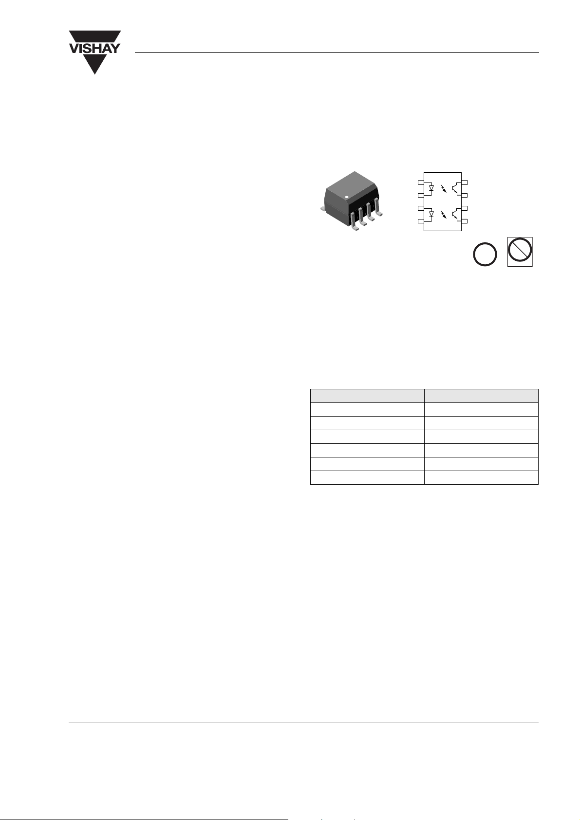
i179018
A1
C2
A3
C4
8C
7E
6C
5E
Vishay Semiconductors
Optocoupler, Phototransistor Output, Dual Channel, SOIC-8
package
Features
• Two Channel Coupler
• SOIC-8A Surface Mountable Package
• Standard Lead Spacing of .05 "
• Available only on Tape and Reel Option (Conforms to EIA Standard 481-2)
• Isolation Test Voltage, 3000 V
• Compatible with Dual Wave, Vapor Phase and IR
Reflow Soldering
• Lead-free component
RMS
e3
Pb
Pb-free
• Component in accordance to RoHS 2002/95/EC
and WEEE 2002/96/EC
Agency Approvals
• UL1577, File No. E52744 System Code Y
Description
The ILD205T/ 206T/ 207T/ 211T/ 213T/ 217T are
optically coupled pairs with a Gallium Arsenide infrared LED and a silicon NPN phototransistor. Signal
information, including a DC level, can be transmitted
by the device while maintaining a high degree of electrical isolation between input and output. The
ILD205T/ 206T/ 207T/ 211T/ 213T/ 217T come in a
standard SOIC-8A small outline package for surface
mounting which makes it ideally suited for high density applications with limited space. In addition to eliminating through-holes requirements, this package
conforms to standards for surface mounted devices.
A specified minimum and maximum CTR allows a
narrow tolerance in the electrical design of the adjacent circuits. The high BV
of 70 V gives a higher
CEO
safety margin compared to the industry standard of
30 V.
Order Information
Part Remarks
ILD205T CTR 40 - 80 %, SOIC-8
ILD206T CTR 63 - 125 %, SOIC-8
ILD207T CTR 100 - 200 %, SOIC-8
ILD211T CTR > 20 %, SOIC-8
ILD213T CTR > 100 %, SOIC-8
ILD217T CTR > 100 %, SOIC-8
For additional information on the available options refer to
Option Information.
Document Number 83647
Rev. 1.4, 26-Oct-04
www.vishay.com
1
Page 2
ILD205T/ 206T/ 207T/ 211T/ 213T/ 217T
Vishay Semiconductors
Absolute Maximum Ratings
T
= 25 °C, unless otherwise specified
amb
Stresses in excess of the absolute Maximum Ratings can cause permanent damage to the device. Functional operation of the device is
not implied at these or any other conditions in excess of those given in the operational sections of this document. Exposure to absolute
Maximum Rating for extended periods of the time can adversely affect reliability.
Input
Parameter Test condition Symbol Val ue Unit
Peak reverse voltage V
Peak pulsed current 1.0 µs, 300 pps 1.0 A
Continuous forward current per
channel
Power dissipation P
Derate linearly from 25 °C 0.66 mW/°C
R
diss
Output
Para meter Test condition Symbol Val ue Unit
Collector-emitter breakdown voltage BV
Emitter-collector breakdown voltage BV
Power dissipation per channel P
Derate linearly from 25 °C 1.67 mW/°C
CEO
ECO
diss
6.0 V
30 mA
50 mW
70 V
7.0 V
125 mW
Coupler
Parameter Test condition Symbol Val ue Unit
Total package dissipation
ambient (2 LEDs + 2 detectors,
2 channels)
Derate linearly from 25 °C 4.0 mW/°C
Storage temperature T
Operating temperature T
Soldering time from 260 °C T
P
tot
stg
amb
sld
300 mW
- 55 to + 150 °C
- 55 to + 100 °C
10 sec.
Electrical Characteristics
T
= 25 °C, unless otherwise specified
amb
Minimum and maximum values are testing requirements. Typical values are characteristics of the device and are the result of engineering
evaluation. Typical values are for information only and are not part of the testing requirements.
Input
Parameter Test condition Symbol Min Ty p. Max Unit
Forward voltage I
Reverse current V
Capacitance V
= 10 mA V
F
= 6.0 V I
R
= 0 C
R
F
R
O
1.2 1.55 V
0.1 100 µA
25 pF
www.vishay.com
2
Document Number 83647
Rev. 1.4, 26-Oct-04
Page 3
ILD205T/ 206T/ 207T/ 211T/ 213T/ 217T
Output
Parameter Test condition Symbol Min Ty p . Max Unit
Collector-emitter breakdown
voltage
Emitter-collector breakdown
voltage
Collector-emitter leakage
current
Collector-emitter capacitance V
Coupler
Parameter Test condition Symbol Min Ty p . Max Unit
Collector-emitter saturation
voltage
Capacitance (input-output) C
Isolation test voltage t = 1.0 sec. V
Resistance, input to output R
Current Transfer Ratio
Parameter Test condition Par t Symbol Min Ty p. Max Unit
DC Current Transfer Ratio V
= 10 µABV
I
C
= 10 µABV
I
E
= 10 V, IF = 0 I
V
CE
= 0 C
CE
= 10 mA, IC = 2.5 mA V
I
F
= 5.0 V, IF = 10 mA ILD205T CTR
CE
ILD206T CTR
ILD207T CTR
ILD211T CTR
ILD213T CTR
V
= 5.0 V, IF = 1.0 mA ILD205T CTR
CE
ILD206T CTR
ILD207T CTR
ILD217T CTR
CEO
ECO
CEO
CE
CE(sat)
IO
ISO
IO
Vishay Semiconductors
70 V
7.0 V
5.0 50 nA
10 pF
0.4 V
0.5 pF
3000 V
100 GΩ
DC
DC
DC
DC
DC
DC
DC
DC
DC
40 80 %
63 125 %
100 200 %
20 %
100 %
13 30 %
22 45 %
34 70 %
100 120 %
RMS
Document Number 83647
Rev. 1.4, 26-Oct-04
www.vishay.com
3
Page 4

ILD205T/ 206T/ 207T/ 211T/ 213T/ 217T
iild205t_03
NCTRce - Normalized CTRce
.01 .1 1 10 100
1.2
1.0
0.8
0.6
0.4
0.2
0.0
IF- LED Current - (mA)
VCE=5 V
CTR normalized @
IF=10mA
VCE=0.4 V
iild205t_04
20 40 60 80 100
1.2
1.0
0.8
0.6
0.4
0.2
0.0
TA- Temperature (°C)
NCTRce - normalized CTRce
IF=5 mA
IF=1 mA
IF=10 mA
CTR nonsat normalized @
I
F
=10 mA
V
CE
=10 V
Vishay Semiconductors
Switching Characteristics
Parameter Test condition Symbol Min Ty p. Max Unit
Turn-on time I
Turn-off time I
= 2.0 mA, RL = 100 Ω,
C
= 5.0 V
V
CC
= 2.0 mA, RL = 100 Ω,
C
= 5.0 V
V
CC
Typical Characteristics (Tamb = 25 °C unless otherwise specified)
If - LED Current (ma)
t
on
t
off
5.0 µs
4.0 µs
iild205t_01
Vf - LED Forward Voltage (V)
Figure 1. Forward Current vs. Forward Voltage
1.2
Coll current normalized @ IF=10 mA
V
=10 V
CE
0246 81012
VCE-Collector to Emitter Voltage (V)
IF=10 mA
I
=5 mA
F
IF=1 mA
NIc Normalized Collector Current
iild205t_02
1.0
0.8
0.6
0.4
0.2
0.0
Figure 2. Collector-Emitter Current vs. Temperature
Figure 3. Normalized CTRce vs. Forward Current
Figure 4. Current Transfer Ratio (normalized) vs. Ambient
Temperature
www.vishay.com
4
Document Number 83647
Rev. 1.4, 26-Oct-04
Page 5

3
iild205t_07
200
150
100
50
0
TA- Ambient Temperature (°C)
Package Power Dissipation (mw)
25 50 75 100 125
Total pkg
per channel
10
IF=10 mA
Pulse width=100 ms
Duty cycle=50%
2
10
ILD205T/ 206T/ 207T/ 211T/ 213T/ 217T
Vishay Semiconductors
To f f
1
10
Switching speed (µs)
0
10
.1 1 10 100
Rl - Load Resistor (KΩ)ˇ
iild205t_01
Figure 5. Switching Speed vs. Load Resistor
Vce=50 V
Vce=50 V
Iceo-Leakage Current - (µa)
iild205t_06
Ta - Temperature (°C)
To n
Figure 7. Power Dissipation vs. Ambient Temperature
Figure 6. Collector Current vs. Ambient Temperature
Input
VCC=5 V
t
pdon
Input
R
V
L
OUT
Output
10%
50%
90%
iild205t_08
Document Number 83647
Rev. 1.4, 26-Oct-04
t
on
t
t
r
d
Figure 8. Switching Test Circuit
t
pdoff
t
off
t
t
s
r
10%
50%
90%
www.vishay.com
5
Page 6

ILD205T/ 206T/ 207T/ 211T/ 213T/ 217T
Vishay Semiconductors
Package Dimensions in Inches (mm)
.120±.002
(3.05±.05)
R .010 (.13)
ISO Method A
i178020
.240
(6.10)
Pin One I.D.
.004 (.10)
.008 (.20)
.040 (1.02)
.230±.002
(5.84±.05)
.050(1.27) Typ.
.154±.002
C
L
(3.91±.05)
.016 (.41)
.050 (1.27)
.015±.002
(.38±.05)
.008 (.20)
.020±.004
(.51±.10)
2 Plcs.
.170 (4.32)
.260 (6.6)
40°
5° Max.
R.010
(.25) Max.
.014 (.36)
.036 (.91)
.045 (1.14)
7°
.0585±.002
(1.49±.05)
.125±.002
(3.18±.05)
Lead coplanarity
±.001 Max.
www.vishay.com
6
Document Number 83647
Rev. 1.4, 26-Oct-04
Page 7

ILD205T/ 206T/ 207T/ 211T/ 213T/ 217T
Vishay Semiconductors
Ozone Depleting Substances Policy Statement
It is the policy of Vishay Semiconductor GmbH to
1. Meet all present and future national and international statutory requirements.
2. Regularly and continuously improve the performance of our products, processes, distribution and
operatingsystems with respect to their impact on the health and safety of our employees and the public, as
well as their impact on the environment.
It is particular concern to control or eliminate releases of those substances into the atmosphere which are
known as ozone depleting substances (ODSs).
The Montreal Protocol (1987) and its London Amendments (1990) intend to severely restrict the use of ODSs
and forbid their use within the next ten years. Various national and international initiatives are pressing for an
earlier ban on these substances.
Vishay Semiconductor GmbH has been able to use its policy of continuous improvements to eliminate the use
of ODSs listed in the following documents.
1. Annex A, B and list of transitional substances of the Montreal Protocol and the London Amendments
respectively
2. Class I and II ozone depleting substances in the Clean Air Act Amendments of 1990 by the Environmental
Protection Agency (EPA) in the USA
3. Council Decision 88/540/EEC and 91/690/EEC Annex A, B and C (transitional substances) respectively.
Vishay Semiconductor GmbH can certify that our semiconductors are not manufactured with ozone depleting
substances and do not contain such substances.
We reserve the right to make changes to improve technical design
and may do so without further notice.
Parameters can vary in different applications. All operating parameters must be validated for each
customer application by the customer. Should the buyer use Vishay Semiconductors products for any
unintended or unauthorized application, the buyer shall indemnify Vishay Semiconductors against all
claims, costs, damages, and expenses, arising out of, directly or indirectly, any claim of personal
damage, injury or death associated with such unintended or unauthorized use.
Vishay Semiconductor GmbH, P.O.B. 3535, D-74025 Heilbronn, Germany
Telephone: 49 (0)7131 67 2831, Fax number: 49 (0)7131 67 2423
Document Number 83647
Rev. 1.4, 26-Oct-04
www.vishay.com
7
Page 8

Legal Disclaimer Notice
Vishay
Document Number: 91000 www.vishay.com
Revision: 08-Apr-05 1
Notice
Specifications of the products displayed herein are subject to change without notice. Vishay Intertechnology, Inc.,
or anyone on its behalf, assumes no responsibility or liability for any errors or inaccuracies.
Information contained herein is intended to provide a product description only. No license, express or implied, by
estoppel or otherwise, to any intellectual property rights is granted by this document. Except as provided in Vishay's
terms and conditions of sale for such products, Vishay assumes no liability whatsoever, and disclaims any express
or implied warranty, relating to sale and/or use of Vishay products including liability or warranties relating to fitness
for a particular purpose, merchantability, or infringement of any patent, copyright, or other intellectual property right.
The products shown herein are not designed for use in medical, life-saving, or life-sustaining applications.
Customers using or selling these products for use in such applications do so at their own risk and agree to fully
indemnify Vishay for any damages resulting from such improper use or sale.
 Loading...