

Page 1
IL74/ ILD74/ ILQ74
i179015
1
2
3
6
5
4
B
C
E
A
C
NC
1
2
3
4
8
7
6
5
E
C
C
E
A
C
C
A
A
C
C
A
A
C
C
A
E
C
C
E
E
C
C
E
16
15
14
13
12
11
10
9
1
2
3
4
5
6
7
8
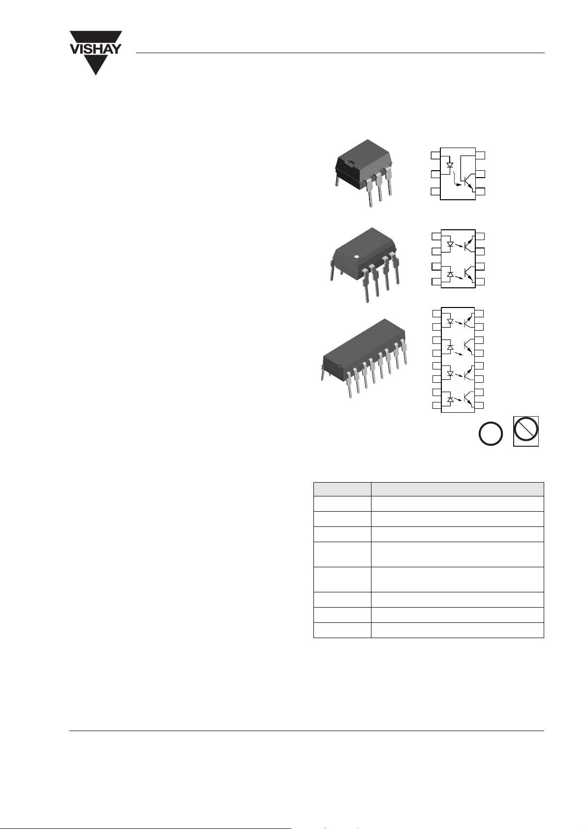
Single Channel
Dual Channel
Quad Channel
Vishay Semiconductors
Optocoupler, Phototransistor Output (Single, Dual, Quad
Channel)
Features
• IL74/ ILD74/ ILQ74 TTL Compatible
• Transfer Ratio, 35 % Typical
• Coupling Capacitance, 0.5 pF
• Single, Dual, & Quad Channel
• Industry Standard DIP Package
• Lead-free component
• Component in accordance to RoHS 2002/95/EC
and WEEE 2002/96/EC
Agency Approvals
• UL1577, File No. E52744 System Code H or J,
Double Protection
• CSA 93751
• BSI IEC60950 IEC60065
• DIN EN 60747-5-2 (VDE0884)
DIN EN 60747-5-5 pending
Available with Option 1, X001 Suffix
• FIMKO
Description
The IL74/ ILD74/ ILQ74 is an optically coupled pair
with a GaAIAs infrared LED and a silicon NPN phototransistor. Signal information, including a DC level,
can be transmitted by the device while maintaining a
high degree of electrical isolation between input and
output.The IL74/ ILD74/ ILQ74 is especially for driving
medium-speed logic, where it may be used to eliminate troublesome ground loop and noise problems.
Also it can be used to replace relays and transformers
in many digital interface applications, as well as analog applications such as CTR modulation.
The ILD74 has two isolated channels in a single DIP
package; the ILQ74 has four isolated channels per
package.
Document Number 83640
Rev. 1.4, 26-Oct-04
e3
Order Information
Part Remarks
IL74 CTR
ILD74 CTR
ILQ74 CTR
IL74-X006 CTR
ILD74-X006 CTR
ILD74-X007 CTR
ILD74-X009 CTR
ILQ74-X009 CTR
For additional information on the available options refer to
Option Information.
35 %, Single Channel DIP-6
DC
35 %, Dual Channel DIP-8
DC
35 %, Quad Channel DIP-16
DC
35 %, Single Channel DIP-6 400 mil
DC
(option 6)
35 %, Dual Channel DIP-8 400 mil
DC
(option 6)
35 %, Dual Channel SMD-8 (option 7)
DC
35 %, Dual Channel SMD-8 (option 9)
DC
35 %, Quad Channel SMD-16 (option 9)
DC
www.vishay.com
Pb
Pb-free
1
Page 2
IL74/ ILD74/ ILQ74
Vishay Semiconductors
Absolute Maximum Ratings
T
= 25 °C, unless otherwise specified
amb
Stresses in excess of the absolute Maximum Ratings can cause permanent damage to the device. Functional operation of the device is
not implied at these or any other conditions in excess of those given in the operational sections of this document. Exposure to absolute
Maximum Rating for extended periods of the time can adversely affect reliability.
Input
(each channel)
Parameter Test condition Symbol Val ue Unit
Peak reverse voltage V
Forward continuous current I
Power dissipation P
R
F
diss
Derate linearly from 55 % 1.33 mW/°C
Output
Para meter Test condition Symbol Valu e Unit
Collector-emitter breakdown voltage BV
Emitter-collector breakdown voltage BV
Collector-base breakdown voltage BV
Power dissipation P
Derate linearly from 25 °C 2.0 mW/°C
CEO
ECO
CBO
diss
3.0 V
60 mA
100 mW
20 V
5.0 V
70 V
150 mW
Coupler
Parameter Test condition Par t Symbol Va lue Unit
Isolation test voltage t = 1.0 sec. V
Isolation resistance VIO = 500 V, TA = 25 °C R
V
= 500 V, TA = 100 °C R
IO
Total package dissipation IL74 P
ILD74 P
ILQ74 P
ISO
IO
IO
tot
tot
tot
Derate linearly from 25 °C IL74 2.7 mW/°C
ILD74 5.33 mW/°C
ILQ74 6.67 mW/°C
Creepage ≥ 7.0 mm
Clearance ≥ 7.0 mm
Storage temperature T
Operating temperature T
stg
amb
Lead soldering time at 260 °C 10 sec.
5300 V
12
≥ 10
11
≥ 10
RMS
200 mW
400 mW
500 mW
- 55 to + 150 °C
- 55 to + 100 °C
Ω
Ω
www.vishay.com
2
Document Number 83640
Rev. 1.4, 26-Oct-04
Page 3
IL74/ ILD74/ ILQ74
Vishay Semiconductors
Electrical Characteristics
T
= 25 °C, unless otherwise specified
amb
Minimum and maximum values are testing requirements. Typical values are characteristics of the device and are the result of engineering
evaluation. Typical values are for information only and are not part of the testing requirements.
Input
Parameter Test condition Symbol Min Ty p. Max Unit
Forward voltage I
Reverse current V
Capacitance V
Output
Parameter Test condition Symbol Min Ty p. Max Unit
Collector-emitter breakdown
voltage
Collector-emitter leakage
current
Collector-emitter capacitance V
= 20 mA V
F
= 3.0 V I
R
= 0 V C
R
= 1.0 mA BV
I
C
= 5.0 V, IF = 0 I
V
CE
= 0, f = 1.0 MHz C
CE
R
CEO
CEO
CE
F
O
20 50 V
1.3 1.5 V
0.1 100 µA
25 pF
5.0 500 nA
10.0 pF
Coupler
Parameter Test condition Symbol Min Ty p. Max Unit
Saturation voltage collectoremitter
Resistance, input to output R
Capacitance (input-output) C
= 2.0 mA, IF = 16 mA V
I
C
Current Transfer Ratio
Parameter Test condition Symbol Min Ty p. Max Unit
DC Current Transfer Ratio I
= 16 mA, VCE = 5.0 V CTR
F
CEsat
IO
IO
DC
0.3 0.5 V
100 GΩ
0.5 pF
12.5 35 %
Document Number 83640
Rev. 1.4, 26-Oct-04
www.vishay.com
3
Page 4

IL74/ ILD74/ ILQ74
iil74_03
100101.1
0.0
0.5
1.0
1.5
NCTR(SAT)
NCTR
IF- LED Current - mA
NCTR - Normalized CTR
ˇ
Normalized to:
VCE=10V,IF= 10 mA, TA= 25°C
TA= 50°C
CTRce(sat) VCE= 0.4 V
iil74_04
100101.1
0.0
0.5
1.0
1.5
I
F
- LED Current - mA
NCTR(SAT)
NCTR
Normalized to:
VCE=10V,IF=10mA
TA= 25°C
CTRce(sat) VCE= 0.4 V
TA= 70°C
NCTR - Normalized CTR
Vishay Semiconductors
Switching Characteristics
Parameter Test condition Symbol Min Ty p. Max Unit
Switching times R
= 100 Ω, VCE = 10 V,
L
= 2.0 mA
I
C
Typical Characteristics (Tamb = 25 °C unless otherwise specified)
1.4
3
iil74_01
1.
1.2
1.1
1.0
0.9
0.8
VF - Forward Voltage - V
0.7
Ta = –55°C
Ta = 25°C
Ta = 85°C
100101.1
IF - Forward Current - mA
t
, t
on
off
3.0 µs
Figure 1. Forward Voltage vs. Forward Current
1.5
Normalized to:
VCE=10V,IF=10mA
TA= 25°C
1.0
CTRce(sat) VCE= 0.4 V
0.5
NCTR - Normalized CTR
0.0
IF- LED Current - mA
iil74_02
NCTR(SAT)
NCTR
100101.1
Figure 2. Normalized Non-Saturated and Saturated CTR vs. LED
Current
Figure 3. Normalized Non-Saturated and Saturated CTR vs. LED
Current
Figure 4. Normalized Non-Saturated and Saturated CTR vs. LED
Current
www.vishay.com
4
Document Number 83640
Rev. 1.4, 26-Oct-04
Page 5

1.5
iil74_08
.1 1 10 100
0.0
0.5
1.0
1.5
25°C
50°C
70°C
IF - LED Current - mA
NCTRcb - Normalized CTRcb
Normalized to:
IF =10 mA
Vcb = 9.3 V
Ta = 25°C
iil74_09
100
101.1
.01
.1
1
10
100
1000
IF - LED Current - mA
Icb - Collector Base
Photocurrent - µA
Icb = 1.0357 *IF ^1.3631
Ta = 25°C
iil74_10
100
10
1
.1
.01
.1
1
10
NIB-Ta=-20°C
NIb,Ta=25°C
NIb,Ta=50°C
NIb,Ta=70°C
IF- LED Current - mA
Normalized Photocurrent
Normalized to:
If=10mA,Ta=25°C
Normalized to:
VCE=10 V,IF= 10 mA, TA= 25°C
CTRce(sat) VCE= 0.4 V
1.0
TA= 85°C
0.5
IL74/ ILD74/ ILQ74
Vishay Semiconductors
NCTR - Normalized CTR
0.0
NCTR(SAT)
NCTR
.1 1 10 100
IF- LED Current - mA
iil74_05
Figure 5. Normalized Non-Saturated and Saturated CTR vs. LED
Current
35
30
25
50°C
20
15
10
- Collector Current - mA
5
CE
I
25°C
85°C
70°C
0
iil74_06
40
IF- LED Current - mA
60503020100
Figure 6. Collector-Emitter Current vs. Temperature and LED
Current
Figure 8. Normalized CTRcb vs. LED Current and Temp.
Figure 9. Collector Base Photocurrent vs. LED Current
5
10
4
10
3
10
2
10
1
- Collector-Emitter - nA
CEO
I
10
10
10
10
0
-1
-2
Typical
TA- Ambient Temperature - °C
iil74_07
Figure 7. Collector-Emitter Leakage Current vs.Temp.
Document Number 83640
Rev. 1.4, 26-Oct-04
Vce=10V
100806040200-20
Figure 10. Normalized Photocurrent vs. I
and Temp.
F
www.vishay.com
5
Page 6

IL74/ ILD74/ ILQ74
Vishay Semiconductors
iil74_11
NHFE - Normalized HFE
1.2
1.0
0.8
0.6
0.4
70°C
50°C
25°C
-20°C
1 10 100 1000
Ib - Base Current - µA
Normalized to:
Ib=20µA
Vce=10V
Ta = 25°C
Figure 11. Normalized Non-saturated HFE vs. Base Current and
Temperature
1.5
1.0
0.5
70°C
25°C
- 20°C
Vce=0.4 V
50°C
Normalized to:
VCE=10V
IB=20µA
TA= 25°C
0.0
NHFE(sat) - Normalized Saturated HFE
1 10 100 1000
iil74_12
Ib - Base Current -
µA
Figure 12. Normalized Saturated HFE vs. Base Current and
Temperature
2.5
2.0
1.5
1.0
100101.1
iil74_13
1000
tpLH - Propagation Delay µs
Ta = 25°C, IF = 10 mA
Vcc=5V,Vth=1.5V
100
10
1
tpHL
tpLH
RL - Collector Load Resistor - kΩ
Figure 13. Propagation Delay vs. Collector Load Resistor
tpHL - Propagation Delay µs
www.vishay.com
6
Document Number 83640
Rev. 1.4, 26-Oct-04
Page 7

Package Dimensions in mm
IL74/ ILD74/ ILQ74
Vishay Semiconductors
Package Dimensions in Inches (mm)
pin one ID
i178006
.255 (6.48)
.268 (6.81)
.030 (0.76)
.045 (1.14)
4° typ.
.050 (1.27)
.018 (.46)
.022 (.56)
4
3
5
6
.379 (9.63)
.390 (9.91)
1
2
78
.031 (0.79)
.130 (3.30)
.150 (3.81)
.020 (.51 )
.035 (.89 )
.100 (2.54) typ.
ISO Method A
.300 (7.62)
typ.
10°
3°–9°
.008 (.20)
.012 (.30)
14770
.110 (2.79)
.130 (3.30)
.230(5.84)
.250(6.35)
Document Number 83640
Rev. 1.4, 26-Oct-04
www.vishay.com
7
Page 8

IL74/ ILD74/ ILQ74
Vishay Semiconductors
Package Dimensions in Inches (mm)
87654321
910111213141516
.779 (19.77 )
.790 (20.07)
pin one ID
.255 (6.48)
.265 (6.81)
ISO Method A
4°
.018 (.46)
.022 (.56)
i178007
Option 6
.407 (10.36)
.391 (9.96)
.307 (7.8)
.291 (7.4)
.014 (0.35)
.010 (0.25)
.400 (10.16)
.430 (10.92)
.030 (.76)
.045 (1.14)
.100 (2.54)typ.
.028 (0.7)
MIN.
.031(.79)
Option 7
.300 (7.62)
TYP.
.315 (8.0)
MIN.
.331 (8.4)
MIN.
.406 (10.3)
MAX.
.130 (3.30)
.150 (3.81)
.020(.51)
.035 (.89)
.050 (1.27)
.180 (4.6)
.160 (4.1)
.300 (7.62)
3°–9°
.0040 (.102)
.0098 (.249)
typ.
10°
typ.
.008 (.20)
.012 (.30)
.110 (2.79)
.130 (3.30)
Option 9
.375 (9.53)
.395 (10.03)
.300 (7.62)
ref.
.020 (.51)
.040 (1.02)
.315 (8.00)
min.
.230 (5.84)
.250 (6.35)
.012 (.30) typ.
15° max.
18450
www.vishay.com
8
Document Number 83640
Rev. 1.4, 26-Oct-04
Page 9

IL74/ ILD74/ ILQ74
Vishay Semiconductors
Ozone Depleting Substances Policy Statement
It is the policy of Vishay Semiconductor GmbH to
1. Meet all present and future national and international statutory requirements.
2. Regularly and continuously improve the performance of our products, processes, distribution and
operatingsystems with respect to their impact on the health and safety of our employees and the public, as
well as their impact on the environment.
It is particular concern to control or eliminate releases of those substances into the atmosphere which are
known as ozone depleting substances (ODSs).
The Montreal Protocol (1987) and its London Amendments (1990) intend to severely restrict the use of ODSs
and forbid their use within the next ten years. Various national and international initiatives are pressing for an
earlier ban on these substances.
Vishay Semiconductor GmbH has been able to use its policy of continuous improvements to eliminate the use
of ODSs listed in the following documents.
1. Annex A, B and list of transitional substances of the Montreal Protocol and the London Amendments
respectively
2. Class I and II ozone depleting substances in the Clean Air Act Amendments of 1990 by the Environmental
Protection Agency (EPA) in the USA
3. Council Decision 88/540/EEC and 91/690/EEC Annex A, B and C (transitional substances) respectively.
Vishay Semiconductor GmbH can certify that our semiconductors are not manufactured with ozone depleting
substances and do not contain such substances.
We reserve the right to make changes to improve technical design
and may do so without further notice.
Parameters can vary in different applications. All operating parameters must be validated for each
customer application by the customer. Should the buyer use Vishay Semiconductors products for any
unintended or unauthorized application, the buyer shall indemnify Vishay Semiconductors against all
claims, costs, damages, and expenses, arising out of, directly or indirectly, any claim of personal
damage, injury or death associated with such unintended or unauthorized use.
Vishay Semiconductor GmbH, P.O.B. 3535, D-74025 Heilbronn, Germany
Telephone: 49 (0)7131 67 2831, Fax number: 49 (0)7131 67 2423
Document Number 83640
Rev. 1.4, 26-Oct-04
www.vishay.com
9
Page 10

Legal Disclaimer Notice
Vishay
Document Number: 91000 www.vishay.com
Revision: 08-Apr-05 1
Notice
Specifications of the products displayed herein are subject to change without notice. Vishay Intertechnology, Inc.,
or anyone on its behalf, assumes no responsibility or liability for any errors or inaccuracies.
Information contained herein is intended to provide a product description only. No license, express or implied, by
estoppel or otherwise, to any intellectual property rights is granted by this document. Except as provided in Vishay's
terms and conditions of sale for such products, Vishay assumes no liability whatsoever, and disclaims any express
or implied warranty, relating to sale and/or use of Vishay products including liability or warranties relating to fitness
for a particular purpose, merchantability, or infringement of any patent, copyright, or other intellectual property right.
The products shown herein are not designed for use in medical, life-saving, or life-sustaining applications.
Customers using or selling these products for use in such applications do so at their own risk and agree to fully
indemnify Vishay for any damages resulting from such improper use or sale.
 Loading...