

Page 1
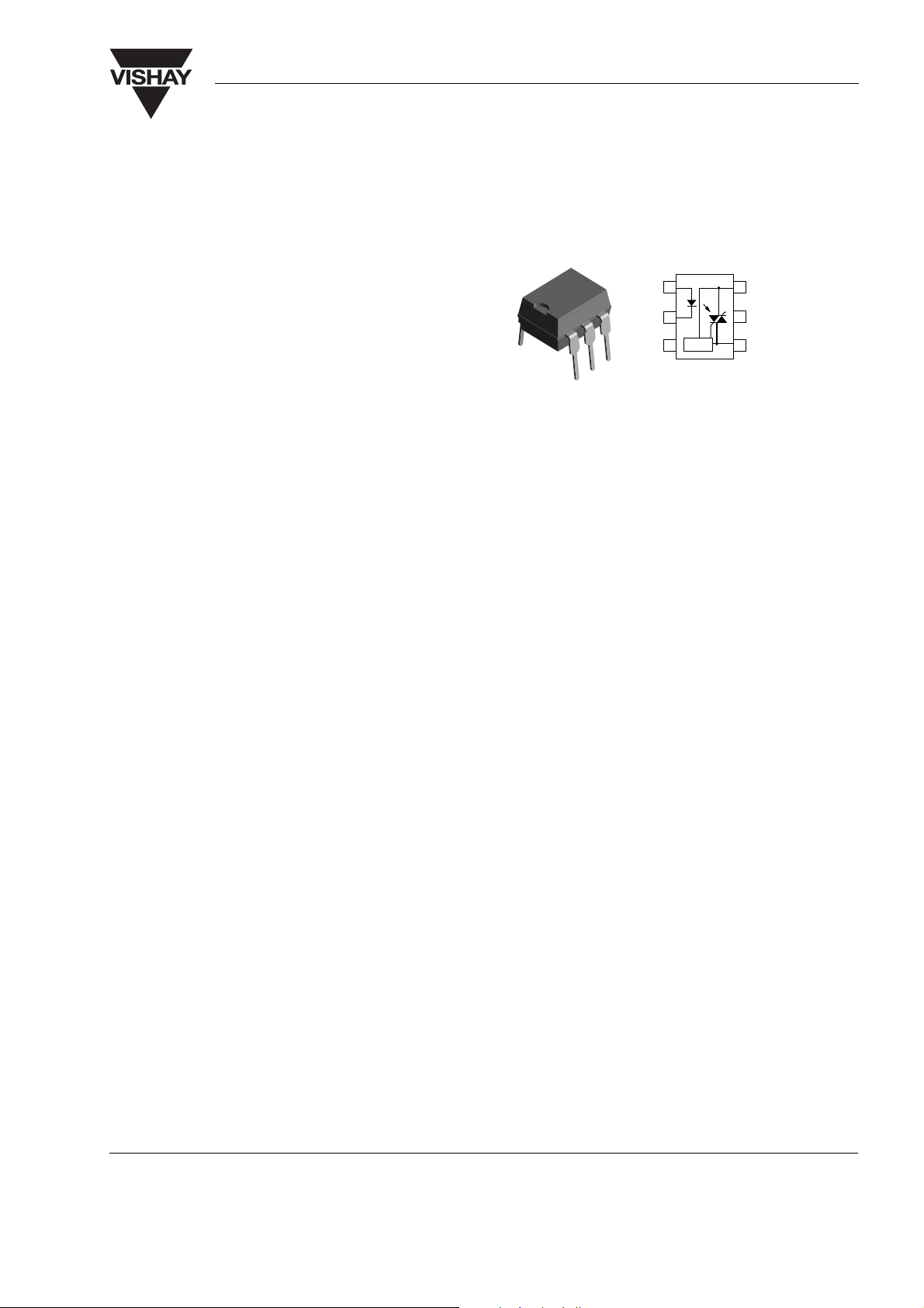
IL410/ IL4108
i179030
1
2
3
6
5
4
MT2
MT1
NC
A
C
NC
*Zero Crossing Circuit
ZCC*
Vishay Semiconductors
Optocoupler, Phototriac Output, Zero Crossing, High dV/dt, Low
Input Current
Features
• High Input Sensitivity
•I
= 2.0 mA, PF = 1.0
FT
•I
= 5.0 mA, PF ≤ 1.0
FT
• 300 mA On-State Current
• Zero Voltage Crossing Detector
• 600/800 V Blocking Voltage
• High Static dV/dt 10 kV/µs
• Inverse Parallel SCRs Provide Commutating
dV/dt >10 kV/µs
• Very Low Leakage < 10 µA
• Isolation Test Voltage 5300 V
RMS
• Small 6-Pin DIP Package
• Lead-free component
• Component in accordance to RoHS 2002/95/EC
and WEEE 2002/96/EC
Agency Approvals
• UL1577, File No. E52744 System Code H or J,
Double Protection
• CSA 93751
• BSI IEC60950 IEC60065
• DIN EN 60747-5-2 (VDE0884)
DIN EN 60747-5-5 pending
Available with Option 1
• FIMKO
Applications
Solid-state relays
Industrial controls
Office equipment
Consumer appliances.
Description
The IL410/ IL4108 consists of a GaAs IRLED optically
coupled to a photosensitive zero crossing TRIAC network. The TRIAC consists of two inverse parallel connected monolithic SCRs. These three semiconductors are assembled in a six pin dual in-line
package.
High input sensitivity is achieved by using an emitter
follower phototransistor and a cascaded SCR predriver resulting in an LED trigger current of less than
2.0 mA (DC).
The IL410/ IL4108 uses two discrete SCRs resulting
in a commutating dV/dt greater than 10 kV/µs. The
use of a proprietary dV/dt clamp results in a static dV/
dt of greater than 10 kV/µs. This clamp circuit has a
MOSFET that is enhanced when high dV/dt spikes
occur between MT1 and MT2 of the TRIAC. When
conducting, the FET clamps the base of the phototransistor, disabling the first stage SCR predriver.
The zero cross line voltage detection circuit consists
of two enhancement MOSFETS and a photodiode.
The inhibit voltage of the network is determined by the
enhancement voltage of the N-channel FET. The Pchannel FET is enabled by a photocurrent source that
permits the FET to conduct the main voltage to gate
on the N-channel FET. Once the main voltage can
enable the N-channel, it clamps the base of the phototransistor, disabling the first stage SCR predriver.
The 600/800 V blocking voltage permits control of offline voltages up to 240 VAC, with a safety factor of
more than two, and is sufficient for as much as
380 VAC.
The IL410/ IL4108 isolates low-voltage logic from
120, 240, and 380 VAC lines to control resistive,
inductive, or capacitive loads including motors, solenoids, high current thyristors or TRIAC and relays.
Document Number 83627
Rev. 1.4, 26-Apr-04
www.vishay.com
1
Page 2
IL410/ IL4108
Vishay Semiconductors
Order Information
Par t Remarks
IL410 600 V V
IL4108 800 V V
IL410-X006 600 V V
IL410-X007 600 V V
IL410-X009 600 V V
IL4108-X006 800 V V
IL4108-X007 800 V V
IL4108-X009 800 V V
For additional information on the available options refer to
Option Information.
Absolute Maximum Ratings
T
= 25 °C, unless otherwise specified
amb
Stresses in excess of the absolute Maximum Ratings can cause permanent damage to the device. Functional operation of the device is
not implied at these or any other conditions in excess of those given in the operational sections of this document. Exposure to absolute
Maximum Rating for extended periods of the time can adversely affect reliability.
, DIP-6
DRM
, DIP-6
DRM
, DIP-6 400 mil (option 6)
DRM
, SMD-6 (option 7)
DRM
, SMD-6 (option 9)
DRM
, DIP-6 400 mil (option 6)
DRM
, SMD-6 (option 7)
DRM
, SMD-6 (option 9)
DRM
Input
Paramete r Test condition Symbol Val ue Unit
Reverse voltage V
Forward current I
Surge current I
Power dissipation P
Derate from 25 °C 1.33 mW/°C
R
F
FSM
diss
6.0 V
60 mA
2.5 A
100 mW
Output
Paramete r Test condition Par t Symbol Val ue Unit
Peak off-state voltage IL410 V
IL4108 V
RMS on-state current I
Single cycle surge current 3.0 A
Total power dissipation P
Derate from 25 °C 6.6 mW/°C
DM
DM
TM
diss
600 V
800 V
300 mA
500 mW
Coupler
Paramete r Test condition Symbol Val ue Unit
Isolation test voltage (between
emitter and detector, climate per
DIN 500414, part 2, Nov. 74)
Pollution degree (DIN VDE
0109)
Creepage ≥ 7.0 mm
Clearance ≥ 7.0 mm
t = 1.0 min. V
ISO
5300 V
2
RMS
www.vishay.com
2
Document Number 83627
Rev. 1.4, 26-Apr-04
Page 3
IL410/ IL4108
Vishay Semiconductors
Parameter Test condition Symbol Value Unit
Comparative tracking index per
DIN IEC 112/VDE 0303 part 1,
group IIIa per DIN VDE 6110
Isolation resistance V
Storage temperature range T
Ambient temperature range T
Soldering temperature max. ≤ 10 sec. dip soldering
= 500 V, T
IO
V
= 500 V, T
IO
= 25 °C R
amb
= 100 °C R
amb
≥ 0.5 mm from case bottom
T
IO
IO
stg
amb
sld
Electrical Characteristics
T
= 25 °C, unless otherwise specified
amb
Minimum and maximum values are testing requirements. Typical values are characteristics of the device and are the result of engineering
evaluation. Typical values are for information only and are not part of the testing requirements.
Input
Parameter Test condition Symbol Min Ty p. Max Unit
Forward voltage I
Reverse current V
Input capacitance V
Thermal resistance, junction to
ambient
= 10 mA V
F
= 6.0 V I
R
= 0 V, f = 1.0 MHz C
F
F
R
IN
R
thja
≥ 175
12
≥ 10
11
≥ 10
- 55 to + 150 °C
- 55 to + 100 °C
260 °C
1.16 1.35 V
0.1 10 µA
25 pF
750 °C/W
Ω
Ω
Output
Parameter Test condition Par t Symbol Min Ty p. Max Unit
Off-state voltage I
Repetitive peak off-state voltage I
Off-state current V
On-state voltage I
On-state current PF = 1.0, V
Surge (non-repetitive), on-state
current
Trigger current 1 V
Trigger current 2 V
Trigger current temp. gradient ∆I
Inhibit voltage temp. gradient ∆V
Off-state current in inhibit state I
Holding current I
Latching current V
Zero cross inhibit voltage I
Turn-on time V
Turn-off time PF = 1.0, I
= 70 µA IL410 V
D(RMS)
IL4108 V
= 100 µA IL410 V
DRM
IL4108 V
= V
, T
D
DRM
I
= 0 mA
F
V
= V
D
DRM
= 300 mA V
T
= 100 °C,
amb
, IF = Rated I
T(RMS)
FT
= 1.7 V I
f = 50 Hz I
= 5.0 V I
D
= 220 V, f = 50 Hz,
OP
T
= 100 °C, tpF > 10 ms
J
∆I
= I
, V
F
FT1
DRM
= 2.2 V I
T
= Rated I
F
RM
FT
= VDM = V
D(RMS)
= 300 mA t
T
D(RMS)
D(RMS)
DRM
DRM
I
D(RMS)1
I
D(RMS)2
TM
TM
TSM
FT1
I
FT2
FT1
FT2
DINH
I
DINH
H
L
V
IH
t
on
off
/∆T
/∆T
/∆T
424 460 V
565 V
600 V
800 V
10 100 µA
1.7 3.0 V
j
j
j
7.0 14 µA/°C
7.0 14 µA/°C
-20 mV/°C
50 200 µA
65 500 µA
5.0 mA
15 25 V
35 µs
50 µs
200 µA
300 mA
3.0 A
2.0 mA
6.0 mA
Document Number 83627
Rev. 1.4, 26-Apr-04
www.vishay.com
3
Page 4
IL410/ IL4108
iil410_01
400350300250200150100500
.001
.01
.1
1
IL - Load Current - mA(RMS)
Cs - Shunt Capacitance - µF
Cs(µF) = 0.0032 (µF)* 10^(0.0066IL (mA)
Ta = 25°C, PF = 0.3
IF = 2.0 mA
Vishay Semiconductors
Paramete r Test condition Par t Symbol Min Ty p. Max Unit
Critical rate of rise of off-state
voltage
Critical rate of rise of voltage at
current commutation
Critical rate of rise of on-state dI/dt
Thermal resistance, junction to
ambient
Coupler
Paramete r Test condition Symbol Min Ty p. Max Unit
Critical rate of rise of coupled
input/output voltage
Common mode coupling
capacitance
Capacitance (input-output) f = 1.0 MHz, V
Isolation resistance V
VD = 0.67 V
= 0.67 V
V
D
V
= 0.67 V
D
≤ 15 A/ms, TJ = 25 °C
dI/dt
crq
V
= 0.67 V
D
≤ 15 A/ms, TJ = 80 °C
dI/dt
crq
= 0 A, VRM = VDM = V
I
T
= 500 V, T
IO
V
= 500 V, T
IO
, TJ = 25 °C dV/dt
DRM
, TJ = 80 °C dV/dt
DRM
,
DRM
,
DRM
= 0 V C
IO
= 25 °C R
amb
= 100 °C R
amb
D(RMS)
dV/dt
dV/dt
dVIO/dt 10000 V/µs
C
CM
IO
IO
IO
10000 V/µs
cr
cr
crq
crq
cr
R
thja
5000 V/µs
10000 V/µs
5000 V/µs
8.0 A/µs
150 °C/W
0.01 pF
0.8 pF
≥ 10
≥ 10
12
11
Ω
Ω
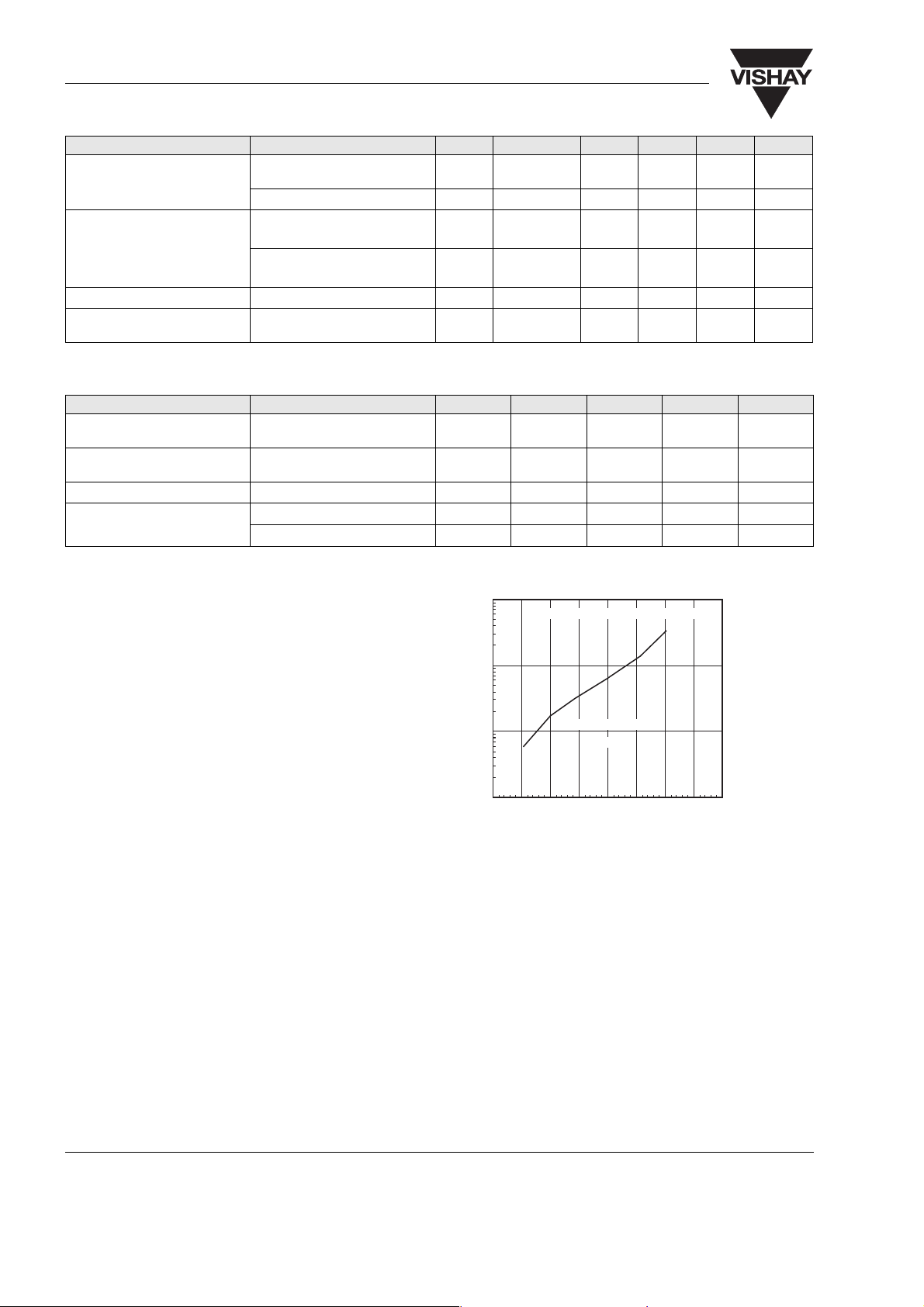
Power Factor Considerations
A snubber isn’t needed to eliminate false operation of
the TRIAC driver because of the IL410/ IL4108’s high
static and commutating dV/dt with loads between 1.0
and 0.8 power factors. When inductive loads with
power factors less than 0.8 are being driven, include
a RC snubber or a single capacitor directly across the
device to damp the peak commutating dV/dt spike.
Normally a commutating dV/dt causes a turning-off
device to stay on due to the stored energy remaining
in the turning-off device.
But in the case of a zero voltage crossing optotriac,
the commutating dV/dt spikes can inhibit one half of
the TRIAC from turning on. If the spike potential
exceeds the inhibit voltage of the zero cross detection
circuit, half of the TRIAC will be held-off and not turnon. This hold-off condition can be eliminated by using
a snubber or capacitor placed directly across the
optotriac as shown in Figure 1. Note that the value of
the capacitor increases as a function of the load current.
Figure 1. Shunt Capacitance vs. Load Current
www.vishay.com
4
Document Number 83627
Rev. 1.4, 26-Apr-04
Page 5

IL410/ IL4108
iil410_04
10-610-510-410-310-210-110010
1
10
100
1000
10000
t -LED Pulse Duration -s
If(pk) - Peak LED Current - mA
.005
.05
.02
.01
.1
.2
.5
Duty Factor
t
τ
DF = /t
τ
iil410_05
100806040200-20-40-60
0
50
100
150
Ta - Ambient Temperature - °C
LED - LED Power - mW
Vishay Semiconductors
The hold-off condition also can be eliminated by providing a higher level of LED drive current. The higher
LED drive provides a larger photocurrent which
causes the phototransistor to turn-on before the commutating spike has activated the zero cross network.
power factors of less than 1.0. The curve shows that
if a device requires 1.5 mA for a resistive load, then
1.8 times (2.7 mA) that amount would be required to
control an inductive load whose power factor is less
than 0.3.
Figure 2 shows the relationship of the LED drive for
Typical Characteristics (Tamb = 25 °C unless otherwise specified)
2.0
1.8
1.6
1.4
1.2
Trigger Current
1.0
NIFth - Normalized LED
0.8
iil410_02
Figure 2. Normalized LED Trigger Current vs. Power Factor
IFth Normalized to IFth @ PF = 1.0
PF - Power Factor
Ta = 25°C
1.21.00.80.60.40.20.0
Figure 4. Peak LED Current vs. Duty Factor, Tau
1.4
1.3
1.2
1.1
1.0
0.9
0.8
VF - Forward Voltage - V
0.7
iil410_03
Document Number 83627
Rev. 1.4, 26-Apr-04
Ta = -55°C
Ta = 25°C
Ta = 85°C
100101.1
IF - Forward Current - mA
Figure 3. Forward Voltage vs. Forward Current
Figure 5. Maximum LED Power Dissipation
www.vishay.com
5
Page 6

IL410/ IL4108
Vishay Semiconductors
IT= f(VT),
parameter: T
tgd=f (IFIFT25°C), VD=200 V,
f=40 to 60 Hz, parameter: T
j
j
iil410_06
iil410_07
Figure 6. Typical Output Characteristics
I
=f(TA),
TRMS
R
=150 K/W
thJA
Device switch
soldered in pcb
or base plate.
Figure 7. Current Reduction
iil410_09
iil410_10
Figure 9. Typical Trigger Delay Time
I
=f (IF/IFT25°C),
DINH
V
=600 V, parameter: T
D
j
Figure 10. Typical Inhibit Current
40 to 60 Hz
line operation,
P
=f(I
TRMS
)
tot
iil410_08
www.vishay.com
6
I
=f(T
), R
TRMS
PIN5
Thermocouple measurement must
be performed potentially separated
to A1 and A2. Measuring junction
as near as possible at the case.
thJ–PIN5
=16.5 K/W
Figure 8. Current Reduction
iil410_11
Figure 11. Power Dissipation 40 to 60 Hz Line Operation
Document Number 83627
Rev. 1.4, 26-Apr-04
Page 7

iil410_12
iil410_13
0.1 µF
220 V~
1
2
3
6
5
4
iil410_14
22 nF
220 V~
2
1
3
5
6
4
33 Ω
iil410_15
22 nF
220 V~
1
2
3
5
4
6
500 µH
V
=f(IF/IFT25°C),
DINHmin
parameter: T
Device zero voltage
switch can be triggered
only in hatched area
below Tj curves.
j
IL410/ IL4108
Vishay Semiconductors
Figure 12. Typical Static Inhibit Voltage Limit
Technical Information
Commutating Behavior
The use of a triac at the output creates difficulties in
commutation due to both the built-in coupled thyristor
systems. The triac can remain conducting by parasitic
triggering after turning off the control current. However, if the IL410/4108 is equipped with two separate
thyristor chips featuring high dv/dt strength, no RC circuit is needed in case of commutation.
Current commutation:
The values 100 A/ms with following peak reverse
recovery current > 80 mA should not be exceeded.
Avoiding high-frequency turn-off current
oscillations:
This effect can occur when switching a circuit. Current
oscillations which appear essentially with inductive
loads of a higher winding capacity result in current
commutation and can generate a relatively high peak
reverse recovery current. The following alternating
protective measures are recommended for the individual operating states:
Figure 13. 1- Apply a Capacitor to the Supply Pins at the Load-Side
Figure 14. 2 - Connect a Series Resistor to the Output and Bridge
Both by a Capacitor
Figure 15. 3 - Connect a Choke of Low Winding Cap. in Series,
e.g., a Ringcore Choke, with Higher Load Currents
Note: Measures 2 to 3 are especially required for the load sepa-
Document Number 83627
Rev. 1.4, 26-Apr-04
rated from the IL410/ IL4108 during operation. The above men-
tioned effects do not occur with IL410/ IL4108 circuits which are
www.vishay.com
7
Page 8

IL410/ IL4108
Vishay Semiconductors
connected to the line by transformers and which are not mechani-
cally interrupted.
In such cases as well as in applications with a resistive load the cor-
responding protective circuits can be neglected.
Control And Turn-On Behavior
The trigger current of the IL410/ IL4108 has a positive
temperature gradient. The time which expires from
applying the control current to the turn-on of the load
current is defined as the trigger delay time (t
the whole this is a function of the overdrive meaning
the ratio of the applied control current versus the trigger current (I
). If the value of the control current
F/IFT
corresponds to that of the individual trigger current of
IL410/4108 turn-on delay times amounts to a few milliseconds only. The shortest times of 5.0 to 10 µs can
be achieved for an overdrive greater or equal than 10.
The trigger delay time rises with an increase in temperature.
For very short control current pulses (t
< 500 µs) a
plF
correspondingly higher control current must be used.
Only the IL410/ IL4108 without zero voltage switch is
suitable for this operating mode.
gd
). On
Application Note
• Over voltage protection: A voltage-limiting varistor
(e.g. SIO VS05K250) which directly connected to the
IL410/ IL4108 can protect the component against
overvoltage.
Zero Voltage Switch
The IL410/ IL4108 with zero voltage switch can only
be triggered during the zero crossing the sine AC voltage. This prevents current spikes, e.g. when turningon cold lamps or capacitive loads.
Applications
Direct switching operation: The IL410/ IL4108 switch
is mainly suited to control synchronous motors,
valves, relays and solenoids in Grätz circuits. Due to
the low latching current (500 µA) and the lack of an
RC circuit at the output, very low load currents can
easily be switched.
Indirect switching operation: The IL410/ IL4108
switch acts here as a driver and thus enables the driving of thyristors and triacs of higher performance by
microprocessors. The driving current pulse should not
exceed the maximum permissible surge current of the
IL410/ IL4108. For this reason, the IL410/ IL4108
without zero voltage switch often requires current limiting by a series resistor.
The favorably low latching current in this operating
mode results in AC current switches which can handle
load currents from some milliamperes up to high currents.
www.vishay.com
8
Document Number 83627
Rev. 1.4, 26-Apr-04
Page 9

Package Dimensions in Inches (mm)
IL410/ IL4108
Vishay Semiconductors
.248 (6.30)
.256 (6.50)
.018 (0.46)
.020 (0.51)
i178014
Option 6
.407 (10.36)
.391 (9.96)
.307 (7.8)
.291 (7.4)
.014 (0.35)
.010 (0.25)
.400 (10.16)
.430 (10.92)
.039
(1.00)
Min.
typ .
4°
3
4
5
.335 (8.50)
.343 (8.70)
.028 (0.7)
MIN.
pin one ID
12
6
.048 (1.22)
.052 (1.32)
.033 (0.84) typ.
.033 (0.84) typ.
.100 (2.54) typ
Option 7
.300 (7.62)
TYP.
.315 (8.0)
MIN.
.331 (8.4)
MIN.
.406 (10.3)
MAX.
.130 (3.30)
.150 (3.81)
.180 (4.6)
.160 (4.1)
3°–9°
ISO Method A
.300 (7.62)
.008 (.20)
.012 (.30)
.300–.347
(7.62–8.81)
.0040 (.102)
.0098 (.249)
typ.
18°
.130 (3.30)
.150 (3.81)
Option 9
.375 (9.53)
.395 (10.03)
.300 (7.62)
ref.
.020 (.51)
.040 (1.02)
.315 (8.00)
min.
.012 (.30) typ.
15° max.
18450
Document Number 83627
Rev. 1.4, 26-Apr-04
www.vishay.com
9
Page 10

IL410/ IL4108
Vishay Semiconductors
Ozone Depleting Substances Policy Statement
It is the policy of Vishay Semiconductor GmbH to
1. Meet all present and future national and international statutory requirements.
2. Regularly and continuously improve the performance of our products, processes, distribution and
operatingsystems with respect to their impact on the health and safety of our employees and the public, as
well as their impact on the environment.
It is particular concern to control or eliminate releases of those substances into the atmosphere which are
known as ozone depleting substances (ODSs).
The Montreal Protocol (1987) and its London Amendments (1990) intend to severely restrict the use of ODSs
and forbid their use within the next ten years. Various national and international initiatives are pressing for an
earlier ban on these substances.
Vishay Semiconductor GmbH has been able to use its policy of continuous improvements to eliminate the use
of ODSs listed in the following documents.
1. Annex A, B and list of transitional substances of the Montreal Protocol and the London Amendments
respectively
2. Class I and II ozone depleting substances in the Clean Air Act Amendments of 1990 by the Environmental
Protection Agency (EPA) in the USA
3. Council Decision 88/540/EEC and 91/690/EEC Annex A, B and C (transitional substances) respectively.
Vishay Semiconductor GmbH can certify that our semiconductors are not manufactured with ozone depleting
substances and do not contain such substances.
We reserve the right to make changes to improve technical design
and may do so without further notice.
Parameters can vary in different applications. All operating parameters must be validated for each
customer application by the customer. Should the buyer use Vishay Semiconductors products for any
unintended or unauthorized application, the buyer shall indemnify Vishay Semiconductors against all
claims, costs, damages, and expenses, arising out of, directly or indirectly, any claim of personal
damage, injury or death associated with such unintended or unauthorized use.
Vishay Semiconductor GmbH, P.O.B. 3535, D-74025 Heilbronn, Germany
Telephone: 49 (0)7131 67 2831, Fax number: 49 (0)7131 67 2423
www.vishay.com
10
Document Number 83627
Rev. 1.4, 26-Apr-04
Page 11

Legal Disclaimer Notice
Vishay
Document Number: 91000 www.vishay.com
Revision: 08-Apr-05 1
Notice
Specifications of the products displayed herein are subject to change without notice. Vishay Intertechnology, Inc.,
or anyone on its behalf, assumes no responsibility or liability for any errors or inaccuracies.
Information contained herein is intended to provide a product description only. No license, express or implied, by
estoppel or otherwise, to any intellectual property rights is granted by this document. Except as provided in Vishay's
terms and conditions of sale for such products, Vishay assumes no liability whatsoever, and disclaims any express
or implied warranty, relating to sale and/or use of Vishay products including liability or warranties relating to fitness
for a particular purpose, merchantability, or infringement of any patent, copyright, or other intellectual property right.
The products shown herein are not designed for use in medical, life-saving, or life-sustaining applications.
Customers using or selling these products for use in such applications do so at their own risk and agree to fully
indemnify Vishay for any damages resulting from such improper use or sale.
 Loading...