

Page 1
Vishay Semiconductors
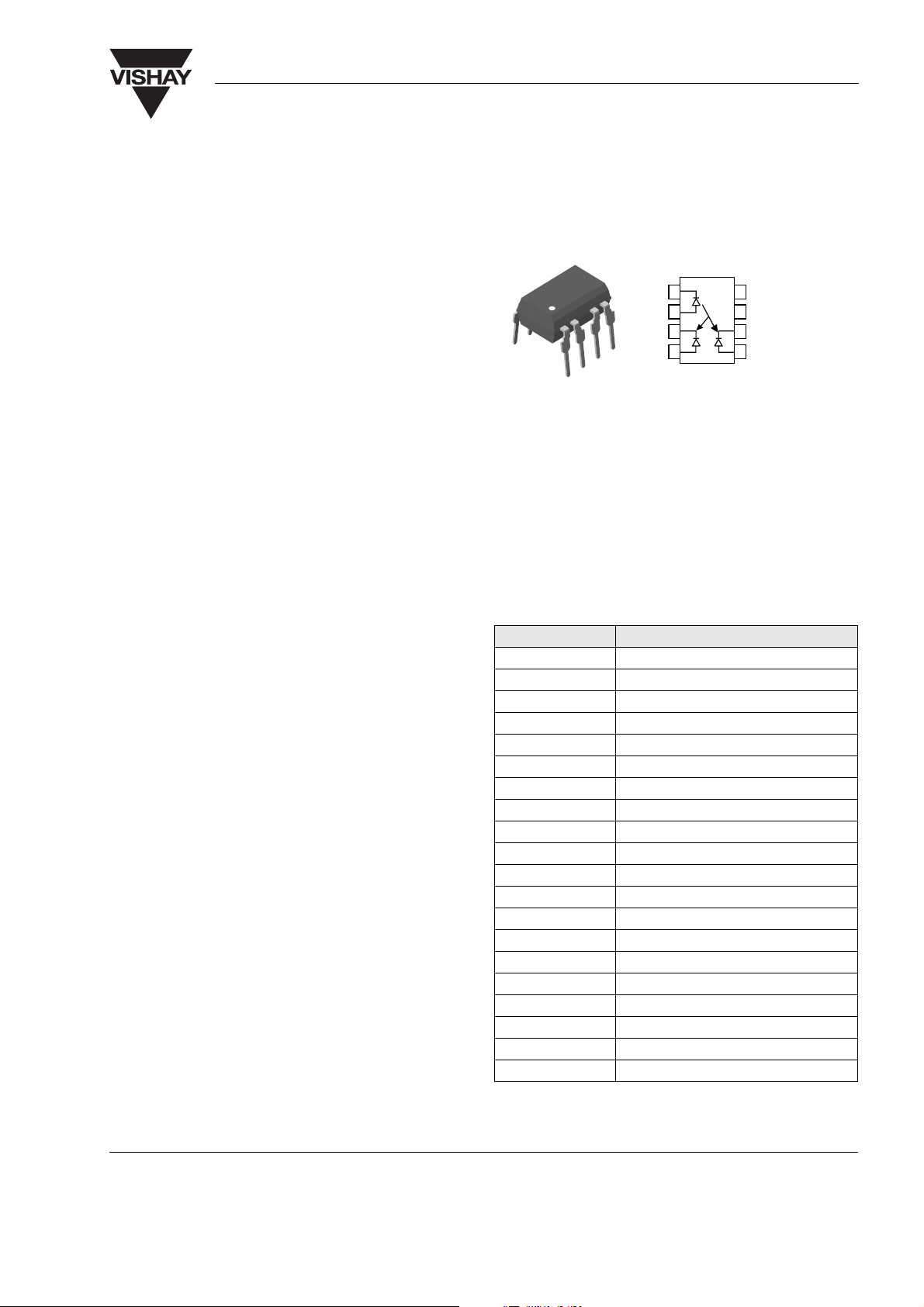
i179026
A
C
NC
NC
C
A
A
C
1
2
3
4
8
7
6
5
K2
K1
Linear Optocoupler, High Gain Stability, Wide Bandwidth
Features
• Couples AC and DC signals
• 0.01 % Servo Linearity
• Wide Bandwidth, > 200 kHz
• High Gain Stability, ± 0.05 %/ °C
• Low Input-Output Capacitance
• Low Power Consumption, < 15 mW
• Isolation Test Voltage, 5300 V
• Internal Insulation Distance, > 0.4 mm for VDE
• Component in accordance to RoHS 2002/95/EC
and WEEE 2002/96/EC
Agency Approvals
• UL File #E52744
• DIN EN 60747-5-2 (VDE0884)
DIN EN 60747-5-5 pending
Available with Option 1, Add -X001 Suffix
RMS
, 1.0 sec.
IL300
Applications
Power Supply Feedback Voltage/Current
Medical Sensor Isolation
Audio Signal Interfacing
Isolated Process Control Transducers
Digital Telephone Isolation
Description
The IL300 Linear Optocoupler consists of an AlGaAs
IRLED irradiating an isolated feedback and an output
PIN photodiode in a bifurcated arrangement. The
feedback photodiode captures a percentage of the
LED’s flux and generates a control signal (I
can be used to servo the LED drive current. This technique compensates for the LED’s non-linear, time,
and temperature characteristics. The output PIN photodiode produces an output signal (I
) that is linearly
P2
related to the servo optical flux created by the LED.
The time and temperature stability of the input-output
coupler gain (K3) is insured by using matched PIN
photodiodes that accurately track the output flux of
the LED.
P1
) that
Order Information
Part Remarks
IL300 K3 = 0.557 - 1.618, DIP-8
IL300-DEFG K3 = 0.765 - 1.181, DIP-8
IL300-EF K3 = 0.851 - 1.061, DIP-8
IL300-E K3 = 0.851 - 0.955, DIP-8
IL300-F K3 = 0.945 - 1.061, DIP-8
IL300-X006 K3 = 0.557 - 1.618, DIP-8 400mil (option 6)
IL300-X007 K3 = 0.557 - 1.618, SMD-8 (option 7)
IL300-X009 K3 = 0.557 - 1.618, SMD-8 (option 9)
IL300-DEFG-X006 K3 = 0.765 - 1.181, DIP-8 400 mil (option 6)
IL300-DEFG-X007 K3 = 0.765 - 1.181, SMD-8 (option 7)
IL300-DEFG-X009 K3 = 0.765 - 1.181, SMD-8 (option 9)
IL300-EF-X006 K3 = 0.851 - 1.061, DIP-8 400 mil (option 6)
IL300-EF-X007 K3 = 0.851 - 1.061, SMD-8 (option 7)
IL300-EF-X009 K3 = 0.851 - 1.061, SMD-8 (option 9)
IL300-E-X006 K3 = 0.851 - 0.955, DIP-8 400 mil (option 6)
IL300-E-X007 K3 = 0.851 - 0.955, SMD-8 (option 7)
IL300-E-X009 K3 = 0.851 - 0.955, SMD-8 (option 9)
IL300-F-X006 K3 = 0.945 - 1.061, DIP-8 400 mil (option 6)
IL300-F-X007 K3 = 0.945 - 1.061, SMD-8 (option 7)
IL300-F-X009 K3 = 0.945 - 1.061, SMD-8 (option 9)
For additional information on the available options refer to
Option Information.
Document Number 83622
Rev. 1.5, 24-Mar-05
www.vishay.com
1
Page 2
IL300
Vishay Semiconductors
VISHAY
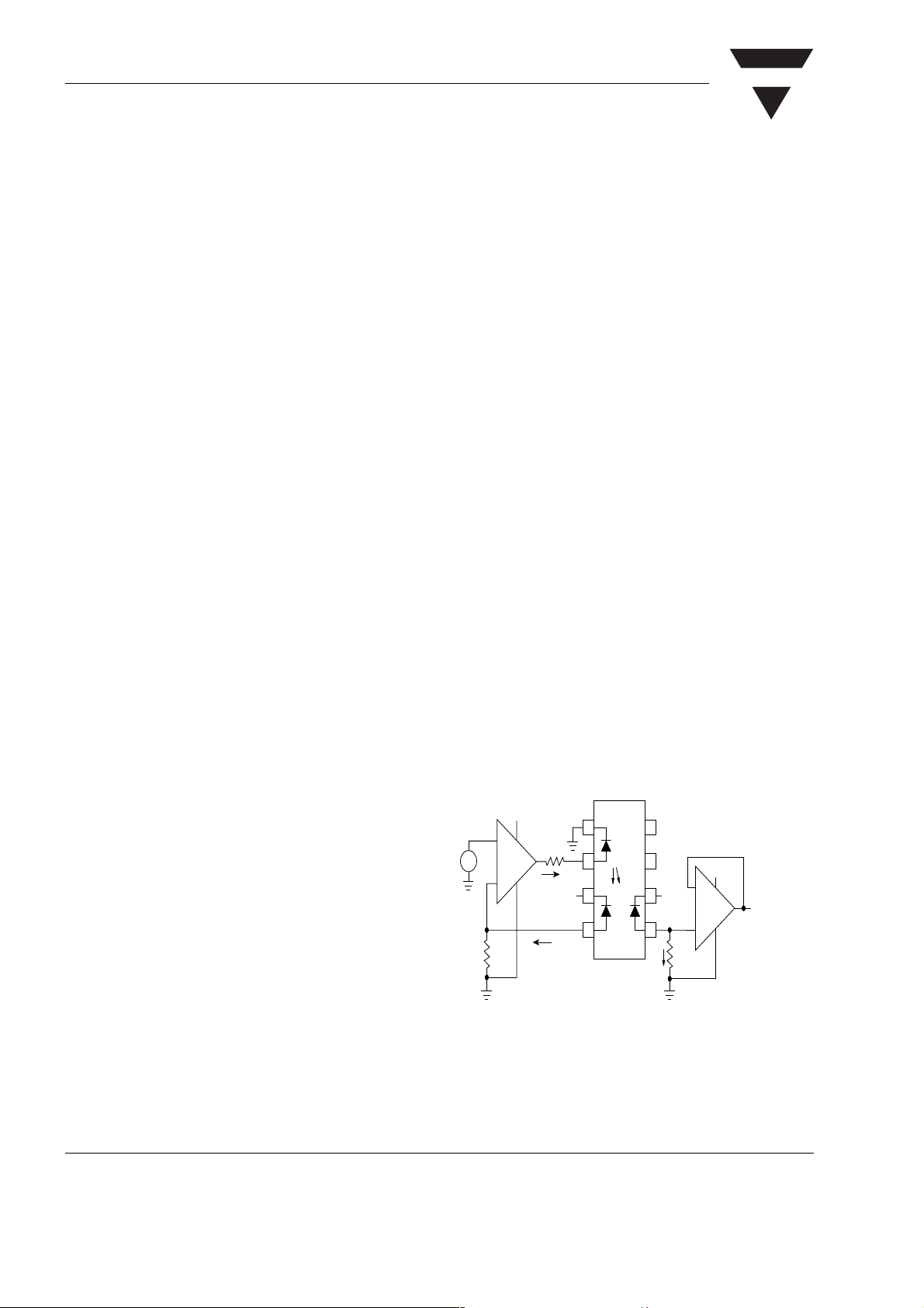
Operation Description
A typical application circuit (Figure 1) uses an operational amplifier at the circuit input to drive the LED.
The feedback photodiode sources current to R1 connected to the inverting input of U1. The photocurrent,
I
, will be of a magnitude to satisfy the relationship of
P1
(I
= VIN/R1).
P1
The magnitude of this current is directly proportional
to the feedback transfer gain (K1) times the LED drive
current ( V
LED current to force sufficient photocurrent to keep
the node voltage (Vb) equal to Va.
The output photodiode is connected to a non-inverting voltage follower amplifier. The photodiode load
resistor, R2, performs the current to voltage conversion. The output amplifier voltage is the product of the
output forward gain (K2) times the LED current and
photodiode load, R2 ( V
Therefore, the overall transfer gain (V
the ratio of the product of the output forward gain (K2)
times the photodiode load resistor (R2) to the product
of the feedback transfer gain (K1) times the input
resistor (R1). This reduces to
V
O/VIN
The overall transfer gain is completely independent of
the LED forward current. The IL300 transfer gain (K3)
is expressed as the ratio of the output gain (K2) to the
feedback gain (K1). This shows that the circuit gain
becomes the product of the IL300 transfer gain times
the ratio of the output to input resistors
V
O/VIN
/R1 = K1 • IF). The op-amp will supply
IN
= IF • K2 • R2).
O
O/VIN
=(K2 • R2)/(K1 • R1).
= K3 (R2/R1).
) becomes
∆K3-Transfer Gain Linearity
The percent deviation of the Transfer Gain, as a function of LED or temperature from a specific Transfer
Gain at a fixed
LED current and temperature.
Photodiode
A silicon diode operating as a current source. The output current is proportional to the incident optical flux
supplied by the LED emitter. The diode is operated in
the photovoltaic or photoconductive mode. In the photovoltaic mode the diode functions as a current
source in parallel with a forward biased silicon diode.
The magnitude of the output current and voltage is
dependent upon the load resistor and the incident
LED optical flux. When operated in the photoconductive mode the diode is connected to a bias supply
which reverse biases the silicon diode. The magnitude of the output current is directly proportional to the
LED incident optical flux.
LED (Light Emitting Diode)
An infrared emitter constructed of AlGaAs that emits
at 890 nm operates efficiently with drive current from
500 µA to 40 mA. Best linearity can be obtained at
drive currents between 5.0 mA to 20 mA. Its output
flux typically changes by - 0.5 % /°C over the above
operational current range.
Application Circuit
K1-Servo Gain
The ratio of the input photodiode current (IP1) to the
LED current (I
) i.e., K1 = IP1/IF.
F
K2-Forward Gain
The ratio of the output photodiode current (IP2) to the
LED current (I
), i.e., K2 = IP2/IF.
F
K3-Transfer Gain
The Transfer Gain is the ratio of the Forward Gain to
the Servo gain, i.e., K3 = K2/K1.
www.vishay.com
2
+
Vin
R1
Va
Vb
V
CC
+
U1
-
I
F
V
CC
lp 1
Figure 1. Typical Application Circuit
IL300
K2
8
7
6
5
lp 2
1
2
K1
3
4
V
CC
-
V
CC
U2
V
c
+
R2
Document Number 83622
Rev. 1.5, 24-Mar-05
V
iil300_01
out
Page 3
VISHAY
IL300
Vishay Semiconductors
Absolute Maximum Ratings
T
= 25 °C, unless otherwise specified
amb
Stresses in excess of the absolute Maximum Ratings can cause permanent damage to the device. Functional operation of the device is
not implied at these or any other conditions in excess of those given in the operational sections of this document. Exposure to absolute
Maximum Rating for extended periods of the time can adversely affect reliability.
Input
Parameter Test condition Symbol Value Unit
Power dissipation P
Derate linearly from 25 °C 2.13 mW/°C
Forward current I
Surge current (pulse width < 10 µs) I
Reverse voltage V
Thermal resistance R
Junction temperature T
diss
F
PK
R
th
j
160 mW
60 mA
250 mA
5.0 V
470 K/W
100 °C
Output
Parameter Test condition Symbol Value Unit
Power dissipation P
Derate linearly from 25 °C 0.65 mW/°C
Reverse voltage V
Junction temperature T
Thermal resistance R
diss
R
j
th
50 mA
50 V
100 °C
1500 K/W
Coupler
Parameter Test condition Symbol Value Unit
Total package dissipation at
25 °C
Derate linearly from 25 °C 2.8 mW/°C
Storage temperature T
Operating temperature T
Isolation test voltage > 5300 V
Isolation resistance VIO = 500 V, T
V
= 500 V, T
IO
= 25 °C R
amb
= 100 °C R
amb
P
amb
tot
stg
IO
IO
210 mW
- 55 to + 150 °C
- 55 to + 100 °C
RMS
12
> 10
11
> 10
Ω
Ω
Document Number 83622
Rev. 1.5, 24-Mar-05
www.vishay.com
3
Page 4
IL300
VISHAY
Vishay Semiconductors
Electrical Characteristics
T
= 25 °C, unless otherwise specified
amb
Minimum and maximum values are testing requirements. Typical values are characteristics of the device and are the result of engineering
evaluation. Typical values are for information only and are not part of the testing requirements.
Input
LED Emitter
Parameter Test condition Symbol Min Ty p. Max Unit
Forward voltage I
Temperature coefficient ∆VF/∆ °C - 2.2 mV/°C
V
F
Reverse current V
Junction capacitance V
Dynamic resistance I
= 10 mA V
F
= 5 V I
R
= 0 V, f = 1.0 MHz C
F
= 10 mA ∆VF/∆I
F
F
R
j
F
1.25 1.50 V
1.0 µA
15 pF
6.0 Ω
Output
Parameter Test condition Symbol Min Ty p. Max Unit
Dark current V
Open circuit voltage I
Short circuit current I
Junction capacitance V
Noise equivalent power V
= -15 V, IF = 0 µsI
det
= 10 mA V
F
= 10 mA I
F
= 0, f = 1.0 MHz C
F
= 15 V NEP
det
D
D
SC
j
1.0 25 nA
500 mV
70 µA
12 pF
14
4 x 10
W/√Hz
www.vishay.com
4
Document Number 83622
Rev. 1.5, 24-Mar-05
Page 5
VISHAY
IL300
Vishay Semiconductors
Coupler
Parameter Test condition Symbol Min Ty p. Max Unit
Input- output capacitance V
K1, Servo gain (I
)I
P1/IF
Servo current, see Note 1,2 I
K2, Forward gain (I
)I
P2/IF
Forward current I
K3, Transfer gain (K2/K1) see
Note 1,2
Transfer gain linearity I
Photoconductive Operation
Frequency response I
Phase response at 200 kHz V
1. Bin Sorting:
K3 (transfer gain) is sorted into bins that are ± 6 % , as follows:
Bin A = 0.557 - 0.626
Bin B = 0.620 - 0.696
Bin C = 0.690 - 0.773
Bin D = 0.765 - 0.859
Bin E = 0.851 - 0.955
Bin F = 0.945 - 1.061
Bin G = 1.051 - 1.181
Bin H = 1.169 - 1.311
Bin I = 1.297 - 1.456
Bin J = 1.442 - 1.618
K3 = K2/K1. K3 is tested at I
F
2. Bin Categories: All IL300s are sorted into a K3 bin, indicated by an alpha character that is marked on the part. The bins range from "A"
through "J".
The IL300 is shipped in tubes of 50 each. Each tube contains only one category of K3. The category of the parts in the tube is marked on
the tube label as well as on each individual part.
3. Category Options: Standard IL300 orders will be shipped from the categories that are available at the time of the order. Any of the ten
categories may be shipped. For customers requiring a narrower selection of bins, four different bin option parts are offered.
IL300-DEFG: Order this part number to receive categories D,E,F,G only.
IL300-EF: Order this part number to receive categories E, F only.
IL300-E: Order this part number to receive category E only.
= 0 V, f = 1.0 MHz 1.0 pF
F
= 10 mA, V
F
= 10 mA, V
F
= 10 mA, V
F
= 10 mA, V
F
= 10 mA, V
I
F
= 1.0 to 10 mA ∆K3 ± 0.25 %
F
I
= 1.0 to 10 mA,
F
= 0 °C to 75 °C
T
amb
= 10 mA, MOD = ± 4.0 mA,
Fq
R
= 50 Ω
L
= - 15 V -45 Deg.
det
= 10 mA, V
det
= - 15 V K1 0.0050 0.007 0.011
det
= - 15 V I
det
= - 15 V K2 0.0036 0.007 0.011
det
= - 15 V I
det
= - 15 V K3 0.56 1.00 1.65 K2/K1
det
P1
P2
70 µA
70 µA
± 0.5 %
BW (-3 db) 200 KHz
= - 15 V.
Switching Characteristics
Parameter Test condition Symbol Min Ty p. Max Unit
Switching time ∆I
Rise time t
Fall tim e t
Document Number 83622
Rev. 1.5, 24-Mar-05
= 2.0 mA, IFq = 10 mA t
F
r
t
f
r
f
1.0 µs
1.0 µs
1.75 µs
1.75 µs
www.vishay.com
5
Page 6

IL300
iil300_04
0°C
25°C
50°C
75°C
V
D
=15V
.1 1 10 100
300
250
200
150
100
50
0
I
F
- LED Current - mA
IP1 - Servo Photocurrent - µA
iil300_05
.1 1 10 100
1000
100
10
1
IF- LED Current - mA
IP1 - Servo Photocurrent - µA
VD= –15 V
0°C
25°C
50°C
75°C
Vishay Semiconductors
Common Mode Transient Immunity
Parameter Test condition Symbol Min Ty p. Max Unit
Common mode capacitance V
Common mode rejection ratio f = 60 Hz, R
= 0, f = 1. MHz C
F
= 2.2 KΩ CMRR 130 dB
L
CM
Typical Characteristics (Tamb = 25 °C unless otherwise specified)
35
30
25
20
15
10
IF - LED Current - mA
5
iil300_02
0
1.0
VF - LED Forward Voltage - V
1.41.31.21.1
0.5 pF
VISHAY
Figure 2. LED Forward Current vs.Forward Voltage
100
10
1
IF - LED Current - mA
.1
1.0 1.1 1.2 1.3 1.4
iil300_03
VF - LED Forward Voltage - V
Figure 3. LED Forward Current vs.Forward Voltage
Figure 4. Servo Photocurrent vs. LED Current and Temperature
Figure 5. Servo Photocurrent vs. LED Current and Temperature
www.vishay.com
6
Document Number 83622
Rev. 1.5, 24-Mar-05
Page 7

VISHAY
iil300_09
.1110100
IF- LED Current - mA
NK1 - Normalized Servo Gain
1.2
1.0
0.8
0.6
0.4
0.2
0.0
0°C
25°C
50°C
75°C
100°C
Normalized to:
IF= 10 mA, TA= 25°C
iil300_10
0 5 10 15 20 25
1.010
1.005
1.000
0.995
0.990
IF- LED Current - mA
K3 - Transfer Gain - (K2/K1)
0°C
25°C
50°C
75°C
iil300_11
0 5 10 15 20 25
1.010
1.005
1.000
0.995
0.990
IF- LED Current - mA
K3 - Transfer Gain - (K2/K1)
0°C
25°C
50°C
75°C
Normalized to:
IF=10mA,
TA= 25°C
3.0
Normalized to: IP1@ IF=10 mA,
2.5
2.0
1.5
1.0
0.5
Normalized Photocurrent
0.0
0 5 10 15 20 25
iil300_06
0°C
25°C
50°C
75°C
IF- LED Current - mA
TA=25°C
VD=–15 V
IL300
Vishay Semiconductors
Figure 6. Normalized Servo Photocurrent vs. LED Current and
Temperature
10
Normalized to: IP1@ IF=10 mA,
0°C
1
.1
IP1 - Normalized Photocurrent
.01
.1 1 10 100
iil300_07
25°C
50°C
75°C
TA=25°C
VD=–15 V
IF- LED Current - mA
Figure 7. Normalized Servo Photocurrent vs. LED Current and
Temperature
NK1 - Normalized Servo Gain
1.2
1.0
0.8
0.6
0.4
0.2
0.0
0°C
25°C
50°C
75°C
85°C
Figure 9. Normalized Servo Gain vs. LED Current and
Temperature
Figure 10. Transfer Gain vs. LED Current and Temperature
.1 1 10 100
iil300_08
IF- LED Current - mA
Figure 8. Servo Gain vs. LED Current and Temperature
Document Number 83622
Rev. 1.5, 24-Mar-05
Figure 11. Normalized Transfer Gain vs. LED Current and
Temperature
www.vishay.com
7
Page 8

IL300
iil300_15
0
2
4
6
8
10
12
14
Voltage - V
det
Capacitance - pF
0246810
Vishay Semiconductors
5
IF=10 mA, Mod = ±2.0 mA (peak)
0
-5
VISHAY
RL=1.0 KΩˇ
-10
-15
Amplitude Response - dB
-20
4
10
F - Frequency - Hz
iil300_12
Figure 12. Amplitude Response vs. Frequency
5
0
-5
-10
IFq=10 mA
Mod= ±4.0 mA
-15
Amplitude Response - dB
iil300_13
CMRR - Rejection Ratio - dB
iil300_14
www.vishay.com
8
TA=25°C
RL=50 Ω
-20
3
10
Figure 13. Amplitude and Phase Response vs. Frequency
-60
-70
-80
-90
-100
-110
-120
-130
10 100 1000 10000 100000 1000000
4
10
F - Frequency - Hz
F - Frequency - Hz
Figure 14. Common-Mode Rejection
10
5
10
dB
PHASE
5
RL=10 KΩˇ
10
6
10
Figure 15. Photodiode Junction Capacitance vs. Reverse Voltage
45
Application Considerations
In applications such as monitoring the output voltage
0
from a line powered switch mode power supply, measuring bioelectric signals, interfacing to industrial
-45
transducers, or making floating current measurements, a galvanically isolated, DC coupled interface
-90
is often essential. The IL300 can be used to construct
an amplifier that will meet these needs.
-135
∅ - Phase Response - °
10
-180
7
6
The IL300 eliminates the problems of gain nonlinearity and drift induced by time and temperature, by monitoring LED output flux.
A PIN photodiode on the input side is optically coupled to the LED and produces a current directly proportional to flux falling on it. This photocurrent, when
coupled to an amplifier, provides the servo signal that
controls the LED drive current.
The LED flux is also coupled to an output PIN photodiode. The output photodiode current can be directly
or amplified to satisfy the needs of succeeding circuits.
Isolated Feedback Amplifier
The IL300 was designed to be the central element of
DC coupled isolation amplifiers. Designing the IL300
into an amplifier that provides a feedback control signal for a line powered switch mode power is quite simple, as the following example will illustrate.
See Figure 17 for the basic structure of the switch
mode supply using the Infineon TDA4918 Push-Pull
Switched Power Supply Control Chip. Line isolation
and insulation is provided by the high frequency
transformer. The voltage monitor isolation will be provided by the IL300.
Document Number 83622
Rev. 1.5, 24-Mar-05
Page 9

VISHAY
µ
IL300
Vishay Semiconductors
The isolated amplifier provides the PWM control signal which is derived from the output supply voltage.
Figure 16 more closely shows the basic function of
the amplifier.
The control amplifier consists of a voltage divider and
a non-inverting unity gain stage. The TDA4918 data
sheet indicates that an input to the control amplifier is
a high quality operational amplifier that typically
requires a +3.0 V signal. Given this information, the
amplifier circuit topology shown in Figure 18 is
selected.
The power supply voltage is scaled by R1 and R2 so
that there is + 3.0 V at the non-inverting input (Va) of
U1. This voltage is offset by the voltage developed by
photocurrent flowing through R3. This photocurrent is
developed by the optical flux
created by current flowing through the LED. Thus as
the scaled monitor voltage (Va) varies it will cause a
change in the LED current necessary to satisfy the differential voltage needed across R3 at the inverting
input.
The first step in the design procedure is to select the
value of R3 given the LED quiescent current (IFq) and
the servo gain (K1). For this design, I
ure 4 shows the servo photocurrent at I
= 12 mA. Fig-
Fq
is found to
Fq
be 100 µA. With this data R3 can be calculated.
The value of R5 depends upon the IL300 Transfer
Gain (K3). K3 is targeted to be a unit gain device,
however to minimize the part to part Transfer Gain
variation, Infineon offers K3 graded into ± 5 % bins.
R5 can determined using the following equation,
R5 =
V
OUT
V
MONITOR
R3(R1 + R2)
•
R2K3
17166
Or if a unity gain amplifier is being designed (VMONITOR = VOUT, R1 = 0), the equation simplifies to:
R5 =
R3
K3
17190
V
R3 =
To Control
Input
iil300_16
3V
b
=
I
100
Figure 16. Isolated Control Amplifier
A
ISO
AMP
+1
=30KΩ
+
-
R1
R2
17164
Voltage
Monitor
For best input offset compensation at U1, R2 will
equal R3. The value of R1 can easily be calculated
from the following.
V
R1=R2
(
MONITOR
V
a
1
)
-
17165
Document Number 83622
Rev. 1.5, 24-Mar-05
www.vishay.com
9
Page 10

IL300
Vishay Semiconductors
VISHAY
iil300_17
110/
220
MAIN
V
monitor
R1
20 KW
R2
30 KW
AC/DC
RECTIFIER
Va
2
Vb
R3
30 KW
3
4
+
U1
LM201
8
7
SWITCH
SWITCH
MODE
REGULATOR
TDA4918
Figure 17. Switching Mode Power Supply
CC
6
R4
100 W
V
1
100 pF
XFORMER
CONTROL
V
CC
1
2
K1
3
4
RECTIFIER
ISOLATED
FEEDBACK
IL300
K2
AC/DC
8
7
6
5
DC OUTPUT
V
CC
V
out
R5
30 KW
To
control
input
iil300_18
Figure 18. DC Coupled Power Supply Feedback Amplifier
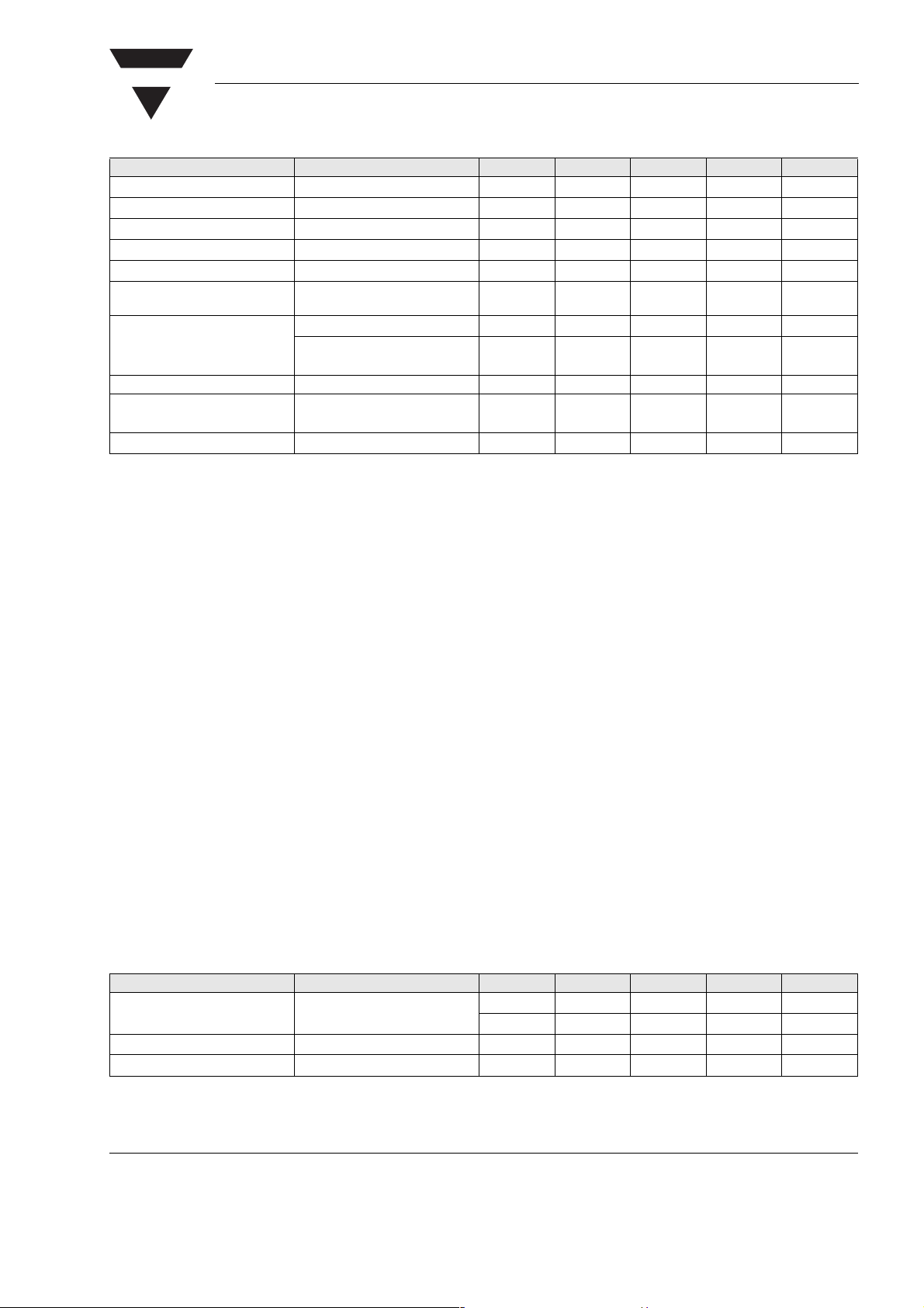
Table 1. gives the value of R5 given the production K3
bins.
R5 Selection
Table 1.
Bins Min. Max. 3
A 0.560 0.623 0.59 50.85 51.1
B 0.623 0.693 0.66 45.45 45.3
C 0.693 0.769 0.73 41.1 41.2
D 0.769 0.855 0.81 37.04 37.4
E 0.855 0.950 0.93 32.26 32.4
F 0.950 1.056 1.00 30.00 30.0
G 1.056 1.175 1.11 27.03 27.0
H 1.175 1.304 1.24 24.19 24.0
I 1.304 1.449 1.37 21.90 22.0
J 1.449 1.610 1.53 19.61 19.4
Ty p.
R5 Resistor
KΩ
1%
KΩ
www.vishay.com
10
Document Number 83622
Rev. 1.5, 24-Mar-05
Page 11

VISHAY
iil300_20
6.05.55.04.54.0
-0.015
-0.010
-0.005
0.000
0.005
0.010
0.015
0.020
0.025
Vin - Input Voltage - V
Linearity Error - %
LM201
iil300_21
dB
PHASE
Phase Response - °
10
3
10
4
10
5
10
6
2
0
-2
-4
-6
-8
45
0
-45
-90
-135
-180
F - Frequency - Hz
Amplitude Response - dB
The last step in the design is selecting the LED current limiting resistor (R4). The output of the operational amplifier is targeted to be 50 % of the V
2.5 V. With an LED quiescent current of 12 mA the
typical LED (V
) is 1.3 V. Given this and the opera-
F
tional output voltage, R4 can be calculated.
CC
, or
IL300
Vishay Semiconductors
R4 =
V
opamp
I
-V
F
2.5 V - 1.3 V
=
12 mA
= 100
Ω
17096
The circuit was constructed with an LM201 differential
operational amplifier using the resistors selected. The
amplifier was compensated with a 100 pF capacitor
connected between pins 1 and 8.
The DC transfer characteristics are shown in Figure
19. The amplifier was designed to have a gain of 0.6
and was measured to be 0.6036. Greater accuracy
can be achieved by adding a balancing circuit, and
potentiometer in the input divider, or at R5. The circuit
shows exceptionally good gain linearity with an RMS
error of only 0.0133 % over the input voltage range of
4.0 V - 6.0 V in a servo mode; see Figure 20.
3.75
3.50
3.25
3.00
2.75
Vout = 14.4 mV + 0.6036 x Vin
LM 201 Ta = 25°C
Figure 20. Linearity Error vs. Input Voltage
The AC characteristics are also quite impressive
offering a - 3.0 dB bandwidth of 100 kHz, with a -45 °
phase shift at 80 kHz as shown in Figure 21.
2.50
Vout - Output Voltage - V
2.25
iil300_19
Document Number 83622
Rev. 1.5, 24-Mar-05
Figure 19. Transfer Gain
6.05.55.04.54.0
Figure 21. Amplitude and Phase Power Supply Control
The same procedure can be used to design isolation
amplifiers that accept bipolar signals referenced to
ground. These amplifiers circuit configurations are
shown in Figure 22. In order for the amplifier to
respond to a signal that swings above and below
ground, the LED must be pre biased from a separate
source by using a voltage reference source (V
ref1
). In
these designs, R3 can be determined by the following
equation.
ref1
V
ref1
=
K1I
17098
www.vishay.com
11
V
R3 =
I
Page 12

IL300
Vishay Semiconductors
Non-Inverting Input Non-Inverting Output
Vin
R1
3
R2
2
–Vref1
+
–
R3
7
4
Vcc
–Vcc
20pF
6
–Vcc
100 Ω
+Vcc
VISHAY
+Vref2
R5
IL 300
1
2
3
4
8
7
Vcc
6
5
R6
2
7
–
Vcc
6
–Vcc
4
Vo
3
+
R4
Inverting Input
R1
iil300_22
Vin
R2
3
+
2
–
R3
+Vref1
7
Vcc
100 Ω
6
+Vcc
Vcc
4
20pF
–Vcc
Table 2. Optolinear amplifiers
Amplifier Input
Inverting
Non-Inverting
Non-Inverting
Inverting Output
IL 300
1
2
3
4
Figure 22. Non-inverting and Inverting Amplifiers
Output Gain Offset
Inverting
Non-Inverting
8
7
6
5
V
OUT
V
V
V
+Vref2
3
+
Vcc
2
–
K3 R4 R2
=
R3 (R1 + R2)
IN
K3 R4 R2 (R5 + R6)
OUT
=
IN
R3 R5 (R1 + R2)
R4
7
Vcc
–Vcc
4
6
Vout
V
ref2
V
ref2
V
R4 K3
ref1
=
R3
R4 (R5 + R6) K3
-V
ref1
=
R3 R6
V
-K3R4R2(R5+R6)
OUT
V
IN
V
V
OUT
IN
=
=
R3 R5 (R1 + R2)
-
K3 R4 R2
R3 (R1 + R2)
Inverting
17189
Inverting
Non-Inverting
Non-Inverting
Inverting
These amplifiers provide either an inverting or noninverting transfer gain based upon the type of input
and output amplifier. Table 2 shows the various configurations along with the specific transfer gain equations. The offset column refers to the calculation of the
output offset or V
www.vishay.com
12
necessary to provide a zero volt-
ref2
V
R4 (R5 + R6) K3
ref1
=
V
V
ref2
ref2
R3 R6
-V
R4 K3
ref1
=
R3
age output for a zero voltage input. The non-inverting
input amplifier requires the use of a bipolar supply,
while the inverting input stage can be implemented
with single supply operational amplifiers that permit
operation close to ground.
Document Number 83622
Rev. 1.5, 24-Mar-05
Page 13

VISHAY
IL300
Vishay Semiconductors
For best results, place a buffer transistor between the
LED and output of the operational amplifier when a
CMOS opamp is used or the LED I
drive is targeted
Fq
to operate beyond 15 mA. Finally the bandwidth is
Package Dimensions in Inches (mm)
.021 (0.527)
.035 (0.889)
6 (.40
.01
.5
(
0
.02
i178010
)
6
)
08
.280 (7.112)
.330 (8.382)
.130 (3.302)
.150 (3.810)
.040 (1.016)
.050 (1.270 )
.020 (0.508) REF.
.008 (0.203)
.012 (0.305)
Pin 1 ID.
1
2
3
4
.380 (9.652)
.400 (10.16)
.300 Typ.
(7.62) Typ.
3°
9
influenced by the magnitude of the closed loop gain of
the input and output amplifiers. Best bandwidths
result when the amplifier gain is designed for unity.
.240 (6.096)
.260 (6.604)
.100 (2.540)
8
7
6
5
10°
4°
.050 (1.270)
.010 (0.254) REF.
.010 (0.254) REF.
ISO Method A
.110 (2.794)
.130 (3.302)
Option 6
.407 (10.36)
.391 (9.96)
.307 (7.8)
.291 (7.4)
.014 (0.35)
.010 (0.25)
.400 (10.16)
.430 (10.92)
Document Number 83622
Rev. 1.5, 24-Mar-05
.028 (0.7)
MIN.
Option 7
.300 (7.62)
TYP.
.315 (8.0)
MIN.
.331 (8.4)
MIN.
.406 (10.3)
MAX.
.180 (4.6)
.160 (4.1)
.0040 (.102)
.0098 (.249)
Option 9
.375 (9.53)
.395 (10.03)
.300 (7.62)
ref.
.020 (.51)
.040 (1.02)
.315 (8.00)
min.
.012 (.30) typ.
15° max.
18450
www.vishay.com
13
Page 14

IL300
VISHAY
Vishay Semiconductors
Ozone Depleting Substances Policy Statement
It is the policy of Vishay Semiconductor GmbH to
1. Meet all present and future national and international statutory requirements.
2. Regularly and continuously improve the performance of our products, processes, distribution and operating
systems with respect to their impact on the health and safety of our employees and the public, as well as
their impact on the environment.
It is particular concern to control or eliminate releases of those substances into the atmosphere which are
known as ozone depleting substances (ODSs).
The Montreal Protocol (1987) and its London Amendments (1990) intend to severely restrict the use of ODSs
and forbid their use within the next ten years. Various national and international initiatives are pressing for an
earlier ban on these substances.
Vishay Semiconductor GmbH has been able to use its policy of continuous improvements to eliminate the use
of ODSs listed in the following documents.
1. Annex A, B and list of transitional substances of the Montreal Protocol and the London Amendments
respectively
2. Class I and II ozone depleting substances in the Clean Air Act Amendments of 1990 by the Environmental
Protection Agency (EPA) in the USA
3. Council Decision 88/540/EEC and 91/690/EEC Annex A, B and C (transitional substances) respectively.
Vishay Semiconductor GmbH can certify that our semiconductors are not manufactured with ozone depleting
substances and do not contain such substances.
We reserve the right to make changes to improve technical design
and may do so without further notice.
Parameters can vary in different applications. All operating parameters must be validated for each
customer application by the customer. Should the buyer use Vishay Semiconductors products for any
unintended or unauthorized application, the buyer shall indemnify Vishay Semiconductors against all
claims, costs, damages, and expenses, arising out of, directly or indirectly, any claim of personal
damage, injury or death associated with such unintended or unauthorized use.
Vishay Semiconductor GmbH, P.O.B. 3535, D-74025 Heilbronn, Germany
www.vishay.com
14
Document Number 83622
Rev. 1.5, 24-Mar-05
Page 15

Legal Disclaimer Notice
Vishay
Document Number: 91000 www.vishay.com
Revision: 08-Apr-05 1
Notice
Specifications of the products displayed herein are subject to change without notice. Vishay Intertechnology, Inc.,
or anyone on its behalf, assumes no responsibility or liability for any errors or inaccuracies.
Information contained herein is intended to provide a product description only. No license, express or implied, by
estoppel or otherwise, to any intellectual property rights is granted by this document. Except as provided in Vishay's
terms and conditions of sale for such products, Vishay assumes no liability whatsoever, and disclaims any express
or implied warranty, relating to sale and/or use of Vishay products including liability or warranties relating to fitness
for a particular purpose, merchantability, or infringement of any patent, copyright, or other intellectual property right.
The products shown herein are not designed for use in medical, life-saving, or life-sustaining applications.
Customers using or selling these products for use in such applications do so at their own risk and agree to fully
indemnify Vishay for any damages resulting from such improper use or sale.
 Loading...