

Page 1

PRODUKTINFORMATION
Vi reserverar oss mot fel samt förbehåller oss rätten till ändringar utan föregående meddelande
ELFA artikelnr
75-352-55 IL205AT Optokopplare
75-352-63 IL207AT Optokopplare
2002-01-04
Page 2
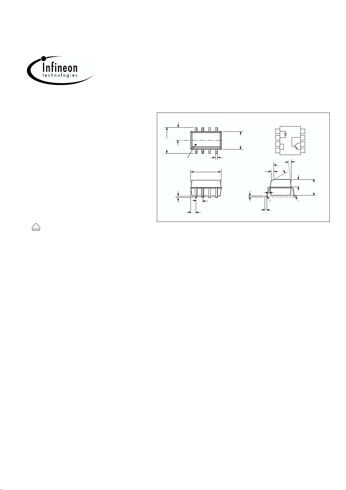
IL205AT/206AT/207AT/208AT
Phototransistor
Small Outline Surface Mount
Optocoupler
Dimensions in inches (mm)
FEATURES
• High Current Transfer Ratio,
I
=10 mA, V
F
CE
=5.0 V
IL205AT, 40–80%
IL206AT, 63–125%
IL207AT, 100–200%
IL208AT, 160–320%
• High BV
• Isolation Test Voltage, 3000 V
CEO
, 70 V
RMS
, 1 s
• Industry Standard SOIC-8A Surface Mountable Package,
• Standard Lead Spacing, .05"
• Compatible with Dual Wave, Vapor Phase and
IR Reflow Soldering
• Underwriters Lab File #E52744 (Code Letter Y)
V
DE
• VDE 0884 Available with Option 1
DESCRIPTION
The IL205AT/206AT/207AT/208AT are optically coupled pairs with a Gallium Arsenide infrared LED
and a silicon NPN phototransistor. Signal information, including a DC level, can be transmitted by the
device while maintaining a high degree of electrical
isolation between input and output. This family
comes in a standard SOIC-8A small outline package for surface mounting which makes them ideally
suited for high density applications with limited
space. In addition to eliminating through-holes
requirements, this package conforms to standards
for surface mounted devices.
A specified minimum and maximum CTR allows a
narrow tolerance in the electrical design of the
adjacent circuits. The high BV
of 70 volts gives
CEO
a higher safety margin compared to the industrystandard 30 volts.
.120±.005
(3.05±.13)
.240
(6.10)
Pin One ID
.192±.005
(4.88±.13)
.004 (.10)
.008 (.20)
.021 (.53)
Maximum Ratings, T
.154±.005
C
L
(3.91±.13)
.016 (.41)
.015±.002
.008 (.20)
.050 (1.27)
typ.
=25 ° C (except where noted)
A
.020±.004
(.51±.10)
(.38±.05)
2 plcs.
Anode
Cathode
NC
NC
1
2
3
4
40°
5° max.
R.010
(.25) max.
8
NC
7
Base
6
Collector
5
Emitter
7°
.058±.005
(1.49±.13)
.125±.005
(3.18±.13)
Lead
Coplanarity
±.0015 (.04)
max.
Emitter
Peak Reverse Voltage ..........................................................................6.0 V
Continuous Forward Current ............................................................. 60 mA
Power Dissipation at 25 ° C.................................................................90 mW
Derate Linearly from 25 ° C .......................................................... 1.2 mW/ ° C
Detector
Collector-Emitter Breakdown Voltage....................................................70 V
Emitter-Collector Breakdown Voltage...................................................7.0 V
Collector-Base Breakdown Voltage.......................................................70 V
I
CMAX DC
I
CMAX
............................................................................................ 50 mA
(t<1.0 ms).............................................................................. 100 mA
Power Dissipation ...........................................................................150 mW
Derate Linearly from 25 ° C .......................................................... 2.0 mW/ ° C
Package
Total Package Dissipation at 25 ° C Ambient
(LED + Detector)..........................................................................240 mW
Derate Linearly from 25 ° C .......................................................... 3.3 mW/ ° C
Operating Temperature .................................................... –55 ° C to +100 ° C
Storage Temperature........................................................ –55 ° C to +150 ° C
Soldering Time at 260 ° C .......................................................................10 s
2001 Infineon Technologies Corp. • Optoelectronics Division • San Jose, CA
www.infineon.com/opto • 1-888-Infineon (1-888-463-4636)
2–107 February 24, 2000-17
Page 3

V
F
d
V
t
V
µ A
=0
Ω
,
µ s
Characteristics, T
=25 ° C
A
Parameter Sym. Min. Typ. Max. Unit Condition
Emitter
Forward Voltage
Reverse Current
Capacitance
V
F
I
R
C
O
— 1.3 1.5 V
— 0.1 100
—13—pF
I
=10 mA
F
=6.0 V
V
R
V
R
Detector
Breakdown Voltage BV
BV
Leakage Current, Collector-Emitter
I
CEO
CEO
ECO
70 — — V
7.0 10 —
— 5.0 50 nA
I
=100 µ A
C
I
=100 µ A
E
=10 V
V
CE
Package
DC
Current
Transfer
IL205AT CTR
DC
40 — 80 %
IL206AT 63 — 125
=10 mA,
I
F
IL207AT 100 — 200
IL208AT 100 — 320
DC
Current
Transfer
IL205AT CTR
DC
13 25 — %
IL206AT 22 40 —
=1.0 mA,
I
F
IL207AT 34 60 —
IL208AT 56 95 —
Saturation Voltage, Collector-Emitter
Isolation Test Voltage
V
CE
sat
V
IO
— — 0.4 —
3000 — — V
RMS
I
=2.0 mA,
C
—
Equivalent DC, Isolation Voltage — 3535 — — VDC —
Capacitance, Input to Output
Resistance, Input to Output
Switching Time
C
IO
R
IO
t
t
ON
OFF
— 0.5 — pF —
— 100 —
— 3.0 —
—
I
=2.0 mA, R
C
V
CE
V
CE
I
=10 mA,
F
=100 Ω ,
L
=5.0 V
=5.0 V
=10 V
V
CC
Figure 1. Forward voltage vs. forward current
Figure 2. Normalized non-saturated and saturated CTR
CE
vs. LED current
1.4
1.3
1.2
age o
orwar
-
F
TA = —55
1.1
TA = 25
1.0
0.9
TA = 85
0.8
0.7
.1 1 10 100
°C
°C
°C
IF - Forward Current - mA
1.5
CE
- Normalized - CTR
CE
NCTR
Normalized to:
=10 V
V
CE
I
=10 mA
F
T
=25
°C
A
1.0
0.5
0.0
.1 1 10 100
- LED Current - mA
I
F
V
VCE =0.4
CE
=5
V
V
2001 Infineon Technologies Corp. • Optoelectronics Division • San Jose, CA IL205AT/206AT/207AT/208AT
www.infineon.com/opto • 1-888-Infineon (1-888-463-4636)
2–108 February 24, 2000-17
Page 4

Figure 3. Collector-emitter current vs. LED curren t
150
TA = 25
°C
= 10 V
V
100
CE
VCE = 0.4 V
50
- Collector-emitter Current - mA
CE
I
0
.1 1 10 100
I
- LED Current - mA
F
Figure 4. Normalized collector-base photo current vs. LED
curren t
100
Normalized to:
=9.3 V
V
10
CB
I
=1 mA
F
T
= 25
°C
A
1
CB
- Normalized I
CB
NI
Figure 6. Collector-emitter photo current vs. LED current
1000
TA = 25
°C
VCB=9.3 V
100
10
1
- Collector-base Current - µA
CB
I
.1
.1 1 10 100
IF - LED Current - mA
Figure 7. Collector-emitter photo current vs. LED current
5
10
4
10
3
10
2
10
1
10
0
10
- Collector-emitter - nA
CEO
-1
I
10
VCE=10 V
Typical
.1
.1 1 10 100
I
- LED Current - mA
F
Figure 5. Normalized collector-base photo current vs. LED
current
10
Normalized to:
=9.3 V
V
CB
- Normalized - I
CB
NI
CB
I
=10 mA
F
T
= 25
°C
A
1
.1
.01
.1 1 10 100
I
- LED Current - mA
F
-2
10
-20 0 20 40 60 80 100
TA - Ambient Temperature - °C
Figure 8. Base current vs. I
2.0
FE
1.5
1.0
FE(sat)
NH
0.5
Normalized Saturated H
0.0
.1 10 100 1000
25
°C
50
°C
25
°C
VCE=0.4 V
I
and HFE
F
- Base Current - µA
B
Normalized to:
I
=20 µA
B
V
=10 V
CE
T
= 25
°C
A
2001 Infineon Technologies Corp. • Optoelectronics Division • San Jose, CA IL205AT/206AT/207AT/208AT
www.infineon.com/opto • 1-888-Infineon (1-888-463-4636)
2–109 February 24, 2000-17
Page 5

Figure 9. Typical switching characteristics
vs. base resistance (saturated operation )
100
Input:
IF=10mA
50
Pulse width=100 mS
Duty cycle=50%
F
F
O
T
10
5
T
Switching time (µs)
ON
1.0
10K 50K 100K 500K 1M
Base-emitter resistance, RBE (Ω)
Figure 10. Typical switching times vs. load
resistance
100
Input:
IF=10mA
50
Pulse width=100 mS
Duty cycle=50%
10
F
F
O
T
Figure 11. Switching time test schematic and waveform
Input
Input
VCC=5 V
R
L
V
OUT
t
pdon
Output
10%
50%
90%
t
on
t
d
t
pdoff
t
r
t
s
t
off
t
r
10%
50%
90%
5
T
Switching time (µs)
ON
1.0
10K 50K 100K 500K 1M
Base-emitter resistance, RBE (Ω)
2001 Infineon Technologies Corp. • Optoelectronics Division • San Jose, CA IL205AT/206AT/207AT/208AT
www.infineon.com/opto • 1-888-Infineon (1-888-463-4636)
2–110 February 24, 2000-17
 Loading...