

Page 1
HFA25TB60SPbF
Vishay High Power Products
Ultrafast Soft Recovery Diode, 25 A
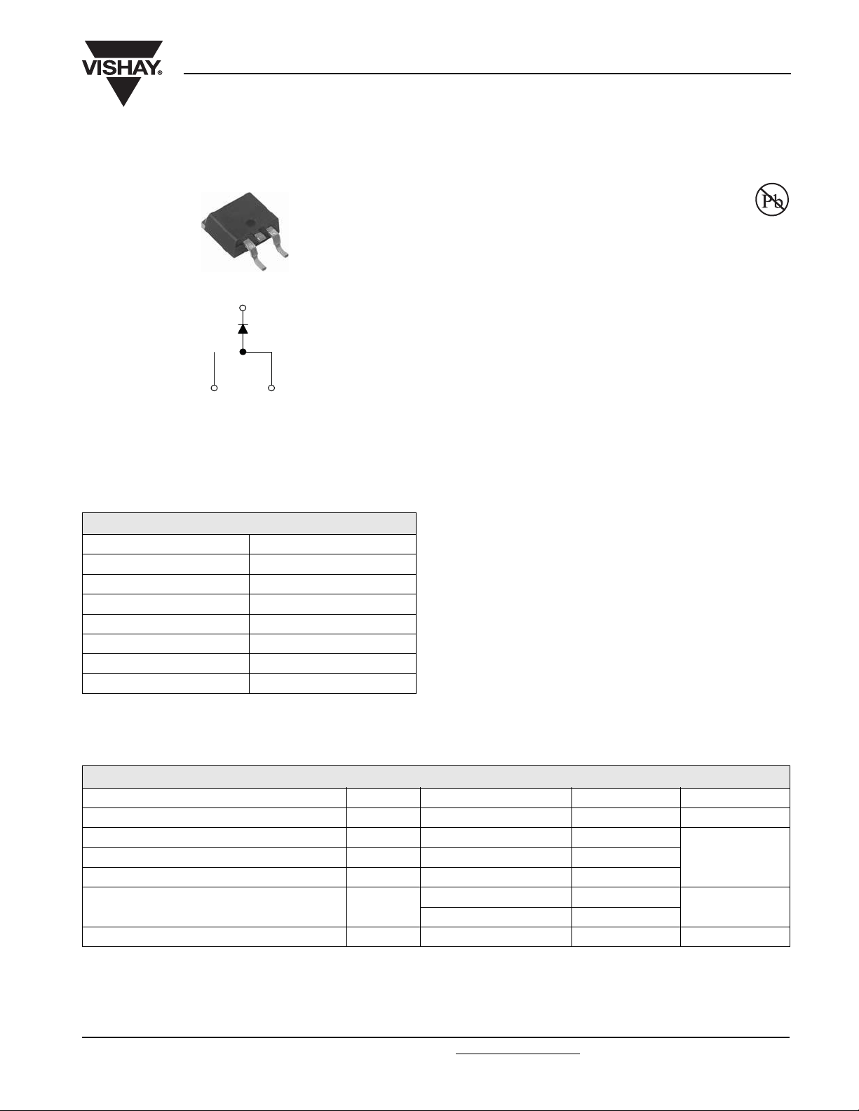
Base
cathode
2
1
N/C
D2PA K
PRODUCT SUMMARY
V
R
V
at 25 A at 25 °C 1.7 V
F
I
F(AV)
(typical) 23 ns
t
rr
T
(maximum) 150 °C
J
Q
(typical) 112 nC
rr
dI
/dt (typical) 250 A/µs
(rec)M
I
RRM
3
Anode
600 V
25 A
10 A
HEXFRED
FEATURES
• Ultrafast recovery
• Ultrasoft recovery
• Very low I
• Very low Q
• Specified at operating conditions
• Lead (Pb)-free
• Designed and qualified for Q101 level
BENEFITS
• Reduced RFI and EMI
• Reduced power loss in diode and switching transistor
• Higher frequency operation
• Reduced snubbing
• Reduced parts count
DESCRIPTION
HFA25TB60S is a state of the art ultrafast recovery diode.
Employing the latest in epitaxial construction and advanced
processing techniques it features a superb combination of
characteristics which result in performance which is
unsurpassed by any rectifier previously available. With basic
ratings of 600 V and 25 A continuous current, the
HFA25TB60S is especially well suited for use as the
companion diode for IGBTs and MOSFETs. In addition to
ultrafast recovery time, the HEXFRED
extremely low values of peak recovery current (I
does not exhibit any tendency to “snap-off” during the
t
portion of recovery. The HEXFRED features combine to
b
offer designers a rectifier with lower noise and significantly
lower switching losses in both the diode and the switching
transistor. These HEXFRED advantages can help to
significantly reduce snubbing, component count and
heatsink sizes. The HEXFRED HFA25TB60S is ideally
suited for applications in power supplies and power
conversion systems (such as inverters), motor drives, and
many other similar applications where high speed, high
efficiency is needed.
®
RRM
rr
Available
RoHS*
COMPLIANT
®
product line features
RRM
) and
ABSOLUTE MAXIMUM RATINGS
PARAMETER SYMBOL TEST CONDITIONS VALUES UNITS
Cathode to anode voltage V
Maximum continuous forward current I
Maximum repetitive forward current I
Maximum power dissipation P
Operating junction and storage temperature range T
* Pb containing terminations are not RoHS compliant, exemptions may apply
Document Number: 94066 For technical questions, contact: diodes-tech@vishay.com
Revision: 25-Jul-08 1
J
F
FSM
FRM
, T
R
TC = 100 °C 25
D
TC = 25 °C 125
T
= 100 °C 50
C
Stg
600 V
225
100
W
- 55 to + 150 °C
www.vishay.com
ASingle pulse forward current I
Page 2
HFA25TB60SPbF
Vishay High Power Products
HEXFRED
®
Ultrafast Soft Recovery Diode, 25 A
ELECTRICAL SPECIFICATIONS (TJ = 25 °C unless otherwise specified)
PARAMETER SYMBOL TEST CONDITIONS MIN. TYP. MAX. UNITS
Cathode to anode
breakdown voltage
Maximum forward voltage V
Maximum reverse
leakage current
V
BR
FM
I
RM
Junction capacitance C
Series inductance L
DYNAMIC RECOVERY CHARACTERISTICS (TJ = 25 °C unless otherwise specified)
PARAMETER SYMBOL TEST CONDITIONS MIN. TYP. MAX. UNITS
t
dI
dI
rr1
t
rr2
I
RRM1
I
RRM2
Q
Q
(rec)M
(rec)M
rr
rr1
rr2
Reverse recovery time
See fig. 5
Peak recovery current
See fig. 6
Reverse recovery charge
See fig. 7
Peak rate of fall recovery
current during t
b
See fig. 8
IR = 100 µA 600 - -
IF = 25 A
I
= 50 A - 1.5 2.0
F
I
= 25 A, TJ = 125 °C - 1.3 1.7
F
VR = VR rated
T
= 125 °C, VR = 0.8 x VR rated - 600 2000
J
VR = 200 V See fig. 3 - 55 100 pF
T
Measured lead to lead 5 mm from package body - 8.0 - nH
S
See fig. 1
See fig. 2
-1.31.7
-1.520
IF = 1.0 A, dIF/dt = 200 A/µs, VR = 30 V - 23 -
TJ = 25 °C
-5075
TJ = 125 °C - 105 160
TJ = 25 °C - 4.5 10
TJ = 125 °C - 8.0 15
TJ = 25 °C - 112 375
TJ = 125 °C - 420 1200
I
= 25 A
F
/dt = 200 A/µs
dI
F
V
= 200 V
R
/dt1 TJ = 25 °C - 250 -
/dt2 TJ = 125 °C - 160 -
V
µA
nst
A
nC
A/µs
THERMAL - MECHANICAL SPECIFICATIONS
PARAMETER SYMBOL TEST CONDITIONS MIN. TYP. MAX. UNITS
Lead temperature T
Thermal resistance,
junction to case
Thermal resistance,
junction to ambient
Weight
Marking device Case style D
www.vishay.com For technical questions, contact: diodes-tech@vishay.com
2 Revision: 25-Jul-08
0.063" from case (1.6 mm) for 10 s - - 300 °C
lead
--1.0
R
thJC
Typical socket mount - - 80
R
thJA
-2.0- g
-0.07- oz.
2
PAK HFA25TB60S
Document Number: 94066
K/W
Page 3

A
A
HFA25TB60SPbF
100
10
HEXFRED
®
Ultrafast Soft Recovery Diode, 25 A
10000
1000
100
10
1
0.1
0.01
0 100 200 300 400 500 600
T = 150°C
J
T = 125°C
J
T = 25°C
J
1000
A
Vishay High Power Products
T = 150°C
J
T = 125°C
J
T = 25°C
J
Reverse Voltage - V (V)
Fig. 2 - Typical Reverse Current vs.
Reverse Voltage
R
1
0.6 1.0 1.4 1.8 2.2 2.6
Forward Voltage Drop - V (V)
FM
Fig. 1 - Maximum Forward Voltage Drop vs.
Instantaneous Forward Current
10
thJC
1
D = 0.50
0.20
0.10
0.1
0.05
0.02
Thermal Response (Z )
0.01
0.01
0.00001 0.0001 0.001 0.01 0.1 1
SINGLE PULSE
(THERMAL RESPONSE)
A
t , Rectangular Pulse Duration (sec)
1
T = 25°C
J
100
10
1 10 100 100
Reverse Voltage - V (V)
R
Fig. 3 - Typical Junction Capacitance vs.
Reverse Voltage
P
DM
t
1
t
2
Notes:
1. Duty factor D = t / t
2. Peak T = P x Z + T
1 2
J DM thJC C
0
Fig. 4 - Maximum Thermal Impedance Z
Characteristics
thJC
Document Number: 94066 For technical questions, contact: diodes-tech@vishay.com
Revision: 25-Jul-08 3
www.vishay.com
Page 4

HFA25TB60SPbF
A
A
A
A
Vishay High Power Products
140
120
100
80
60
40
20
I = 50 A
F
I = 25 A
F
I = 10 A
F
di /dt - (A/µs)
f
V = 200V
R
T = 125°C
J
T = 25°C
J
HEXFRED
®
Ultrafast Soft Recovery Diode, 25 A
1400
V = 200V
R
T = 125°C
J
T = 25°C
J
1200
1000
0001001
800
600
400
200
I = 50 A
F
I = 25 A
F
I = 10 A
F
0
di /dt - (A/µs)
f
0001001
Fig. 5 - Typical Reverse Recovery Time vs. dIF/dt
30
V = 200V
R
T = 125°C
J
T = 25°C
J
25
I = 50 A
F
20
I = 25 A
F
I = 10 A
F
15
10
5
0
di /dt - (A/µs)
f
Fig. 7 - Typical Stored Charge vs. dI
10000
V = 20 0V
R
T = 125°C
J
T = 25°C
J
I = 50 A
100
F
I = 25 A
F
I = 10 A
F
di /dt - (A/µs)
f
1000
0001001
/dt
F
0001001
Fig. 6 - Typical Recovery Current vs. dI
/dt
F
Fig. 8 - Typical dI
/dt vs. dIF/dt
(rec)M
www.vishay.com For technical questions, contact: diodes-tech@vishay.com
4 Revision: 25-Jul-08
Document Number: 94066
Page 5

HFA25TB60SPbF
HEXFRED
®
Ultrafast Soft Recovery Diode, 25 A
V
= 200 V
R
0.01 Ω
L = 70 µH
(3)
a
(2)
D
IRFP250
S
t
rr
I
RRM
(4) Q
and I
(5) dI
current during t
dIF/dt
adjust
G
Fig. 9 - Reverse Recovery Parameter Test Circuit
I
F
0
dIF/dt
(1)
/dt - rate of change of current
(1) dI
F
through zero crossing
- peak reverse recovery current
(2) I
RRM
- reverse recovery time measured
(3) t
rr
from zero crossing point of negative
going I
through 0.75 I
extrapolated to zero current.
to point where a line passing
F
and 0.50 I
RRM
RRM
Fig. 10 - Reverse Recovery Waveform and Definitions
t
Vishay High Power Products
D.U.T.
t
b
(4)
Q
rr
0.5 I
RRM
(rec)M
Q
rr
(5)
/dt
trr x I
=
portion of t
b
RRM
2
rr
dI
0.75 I
RRM
- area under curve defined by t
rr
RRM
/dt - peak rate of change of
(rec)M
rr
LINKS TO RELATED DOCUMENTS
Dimensions http://www.vishay.com/doc?95046
Part marking information http://www.vishay.com/doc?95044
Packaging information http://www.vishay.com/doc?95032
Document Number: 94066 For technical questions, contact: diodes-tech@vishay.com
www.vishay.com
Revision: 25-Jul-08 5
Page 6

Legal Disclaimer Notice
Vishay
Notice
The products described herein were acquired by Vishay Intertechnology, Inc., as part of its acquisition of
International Rectifier’s Power Control Systems (PCS) business, which closed in April 2007. Specifications of the
products displayed herein are pending review by Vishay and are subject to the terms and conditions shown below.
Specifications of the products displayed herein are subject to change without notice. Vishay Intertechnology, Inc., or
anyone on its behalf, assumes no responsibility or liability for any errors or inaccuracies.
Information contained herein is intended to provide a product description only. No license, express or implied, by
estoppel or otherwise, to any intellectual property rights is granted by this document. Except as provided in Vishay's
terms and conditions of sale for such products, Vishay assumes no liability whatsoever, and disclaims any express
or implied warranty, relating to sale and/or use of Vishay products including liability or warranties relating to fitness
for a particular purpose, merchantability, or infringement of any patent, copyright, or other intellectual property right.
The products shown herein are not designed for use in medical, life-saving, or life-sustaining applications.
Customers using or selling these products for use in such applications do so at their own risk and agree to fully
indemnify Vishay for any damages resulting from such improper use or sale.
International Rectifier
are registered trademarks of International Rectifier Corporation in the U.S. and other countries. All other product
names noted herein may be trademarks of their respective owners.
®
, IR®, the IR logo, HEXFET®, HEXSense®, HEXDIP®, DOL®, INTERO®, and POWIRTRAIN
®
Document Number: 99901 www.vishay.com
Revision: 12-Mar-07 1
 Loading...