

HFA180NH40PbF
Vishay High Power Products
Ultrafast Soft Recovery Diode, 180 A
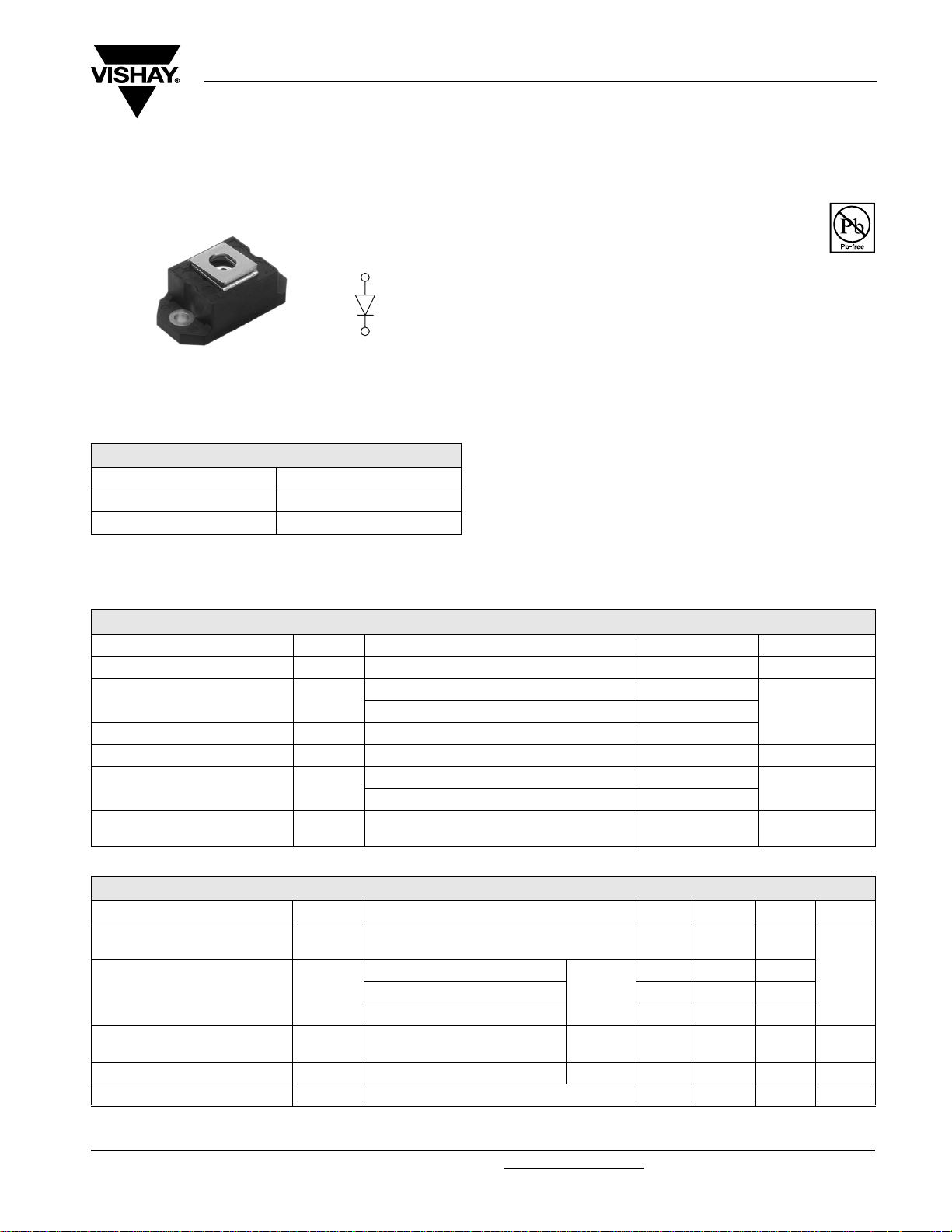
HALF-PAK (D-67)
PRODUCT SUMMARY
I
F(AV)
V
R
I
at T
F(DC)
C
Lug terminal
anode
Base
cathode
180 A
400 V
200 A at 100 °C
HEXFRED
FEATURES
• Very low Qrr and t
• Lead (Pb)-free
• Designed and qualified for industrial level
BENEFITS
• Reduced RFI and EMI
• Reduced snubbing
DESCRIPTION
HEXFRED® diodes are optimized to reduce losses and
EMI/RFI in high frequency power conditioning systems. An
extensive characterization of the recovery behavior for
different values of current, temperature and dI/dt simplifies
the calculations of losses in the operating conditions. The
softness of the recovery eliminates the need for a snubber in
most applications. These devices are ideally suited for
power converters, motors drives and other applications
where switching losses are significant portion of the total
losses.
®
rr
RoHS
COMPLIANT
ABSOLUTE MAXIMUM RATINGS
PARAMETER SYMBOL TEST CONDITIONS MAX. UNITS
Cathode to anode voltage V
Continuous forward current I
Single pulse forward current I
Non-repetitive avalanche energy E
Maximum power dissipation P
Operating junction and storage
temperature range
T
J
F
FSM
AS
, T
R
TC = 25 °C 395
= 100 °C 200
C
Limited by junction temperature 1200
L = 100 µH, duty cycle limited by maximum T
TC = 25 °C 657
D
T
= 100 °C 263
C
Stg
J
400 V
AT
1.4 mJ
W
- 55 to + 150 °C
ELECTRICAL SPECIFICATIONS (TJ = 25 °C unless otherwise specified)
PARAMETER SYMBOL TEST CONDITIONS MIN. TYP. MAX. UNITS
Cathode to anode
breakdown voltage
Maximum forward voltage V
Maximum reverse
leakage current
Junction capacitance C
Series inductance L
V
BR
FM
I
RM
S
IR = 100 µA 400 - -
IF = 180 A
I
= 360 A - 1.22 1.8
F
I
= 180 A, TJ = 125 °C - 0.99 1.34
F
TJ = 125 °C, VR = 400 V See fig. 2 - - 4 mA
VR = 200 V See fig. 3 - 370 500 pF
T
From top of terminal hole to mounting plane - 6.0 - nH
See fig. 1
- 1.08 1.46
V
Document Number: 94061 For technical questions, contact: ind-modules@vishay.com
Revision: 01-Aug-08 1
www.vishay.com
HFA180NH40PbF
Vishay High Power Products
HEXFRED
®
Ultrafast Soft Recovery
Diode, 180 A
DYNAMIC RECOVERY CHARACTERISTICS (TJ = 25 °C unless otherwise specified)
PARAMETER SYMBOL TEST CONDITIONS MIN. TYP. MAX. UNITS
Reverse recovery time
See fig. 5
Peak recovery current
See fig. 6
Reverse recovery charge
See fig. 7
Peak rate of recovery current
See fig. 8
dI
t
rr
I
RRM
Q
(rec)M
TJ = 25 °C
T
= 125 °C - 280 440
J
TJ = 25 °C - 9 16
= 135 A
I
T
= 125 °C - 18 32
J
TJ = 25 °C - 300 950
rr
T
= 125 °C - 2650 6300
J
= 25 °C - 300 -
T
J
/dt
T
= 125 °C - 290 -
J
F
/dt = 200 A/µs
dI
F
V
= 200 V
R
THERMAL - MECHANICAL SPECIFICATIONS
PARAMETER SYMBOL TEST CONDITIONS VALUES UNITS
Maximum junction and storage
temperature range
Maximum thermal resistance,
junction to case
Typical thermal resistance,
case to heatsink
Approximate weight
Mounting torque
Terminal torque
Case style HALF-PAK module
minimum 3 (26.5)
maximum 4 (35.4)
minimum 3.4 (30)
maximum 5 (44.2)
T
, T
J
Stg
DC operation
R
thJC
R
thCS
See fig. 4
Mounting surface, smooth and greased 0.05
- 90 140
- 55 to 150 °C
0.19
°C/W
30 g
1.06 oz.
N · m
(lbf · in)
ns
A
nC
A/µs
www.vishay.com For technical questions, contact: ind-modules@vishay.com
2 Revision: 01-Aug-08
Document Number: 94061
HFA180NH40PbF
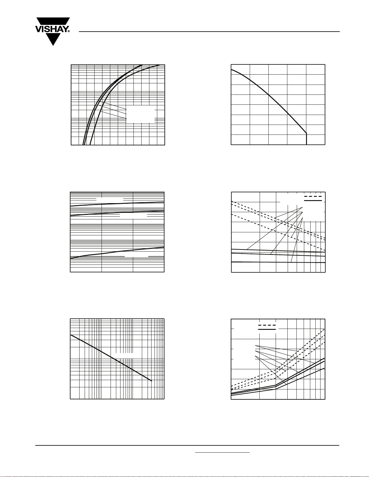
1000
100
10
1
- Instantaneous Forward Current (A)
F
I
0 3.01.0
Fig. 1 - Maximum Forward Voltage Drop vs.
10
1
0.1
0.01
- Reverse Current (µA)
0.001
R
I
0.0001
100
Fig. 2 - Typical Reverse Current vs.
Ultrafast Soft Recovery
TJ = 150 °C
= 125 °C
T
J
= 25 °C
T
J
0.5 2.0
VFM - Forward Voltage Drop (V)
Instantaneous Forward Current
VR - Reverse Voltage (V)
1.5
TJ = 150 °C
TJ = 125 °C
TJ = 25 °C
200 400300
Reverse Voltage
2.5
HEXFRED
®
Diode, 180 A
Vishay High Power Products
160
140
120
100
80
60
Case Temperature (°C)
40
20
0
0 100 300 500
I
- DC Forward Current (A)
F(AV)
Maximum Allowable
Fig. 4 - Maximum Allowable Case Temperature vs. DC
Forward Current
400
350
300
250
200
(ns)
rr
t
150
100
50
0
100
Fig. 5 - Typical Reverse Recovery Time vs. dI
DC
200 400
TJ = 125 °C
TJ = 25 °C
dIF/dt (A/µs)
IF = 200 A
= 180 A
I
F
= 70 A
I
F
1000
F
/dt
(A)
RRM
I
Fig. 6 -
80
TJ = 125 °C
70
TJ = 25 °C
60
IF = 200 A
50
= 180 A
I
F
= 70 A
I
F
40
30
20
10
0
100
dIF/dt (A/µs)
- Typical Recovery Current vs. dIF/dt
1000
10 000
1000
- Junction Capacitance (pF)
T
C
100
1 10 100 1000
TJ = 25 °C
VR - Reverse Voltage (V)
Fig. 3 - Typical Junction Capacitance vs. Reverse Voltage
Document Number: 94061 For technical questions, contact: ind-modules@vishay.com
www.vishay.com
Revision: 01-Aug-08 3

HFA180NH40PbF
Vishay High Power Products
6000
TJ = 125 °C
TJ = 25 °C
5000
0
100
IF = 200 A
= 180 A
I
F
= 70 A
I
F
1
dIF/dt (A/µs)
4000
3000
(nC)
rr
Q
2000
1000
Fig. 7 - - Typical Stored Charge vs. dI
HEXFRED
®
Ultrafast Soft Recovery
Diode, 180 A
10 000
200 A
180 A
70 A
1000
/dt (A/µs)
(rec)M
dI
1000
/dt Fig. 8 - Typical dI
F
100
100
dIF/dt (A/µs)
TJ = 125 °C
TJ = 25 °C
/dt vs. dIF/dt
(rec)M
1000
0.1
0.01
- Thermal Response
thJC
Z
0.001
0.00001 0.0001 0.001 0.01 0.1
Single pulse
(thermal response)
D = 0.50
D = 0.33
D = 0.25
D = 0.17
D = 0.08
t1 - Rectangular Pulse Duration (s)
Fig. 9 - Maximum Thermal Impedance Z
Characteristics
thJC
1
10
www.vishay.com For technical questions, contact: ind-modules@vishay.com
Document Number: 94061
4 Revision: 01-Aug-08

HFA180NH40PbF
HEXFRED
Ultrafast Soft Recovery
Diode, 180 A
L = 70 µH
dIF/dt
adjust
Fig. 10 - Reverse Recovery Parameter Test Circuit
I
F
0
(1)
/dt - rate of change of current
(1) dI
F
through zero crossing
- peak reverse recovery current
(2) I
RRM
- reverse recovery time measured
(3) t
rr
from zero crossing point of negative
going I
through 0.75 I
extrapolated to zero current.
to point where a line passing
F
and 0.50 I
RRM
Fig. 11 - Reverse Recovery Waveform and Definitions
dIF/dt
RRM
G
V
= 200 V
R
®
Vishay High Power Products
0.01 Ω
D.U.T.
D
IRFP250
S
(3)
t
rr
t
a
(2)
I
RRM
t
b
(4)
Q
rr
0.5 I
RRM
dI
/dt
(rec)M
0.75 I
RRM
(4) Q
- area under curve defined by t
rr
and I
RRM
trr x I
(5) dI
current during t
=
Q
rr
/dt - peak rate of change of
(rec)M
portion of t
b
(5)
rr
RRM
2
rr
L = 100 µH
I
L(PK)
High-speed
Freewheel
diode
switch
V
= 50 V
d
+
Decay
time
V
(AVAL)
V
R(RATED)
D.U.T.
Current
monitor
R
g
= 25 Ω
Fig. 12 - Avalanche Test Circuit and Waveforms
Document Number: 94061 For technical questions, contact: ind-modules@vishay.com
www.vishay.com
Revision: 01-Aug-08 5

HFA180NH40PbF
Vishay High Power Products
HEXFRED
®
Ultrafast Soft Recovery
Diode, 180 A
ORDERING INFORMATION TABLE
Device code
Dimensions http://www.vishay.com/doc?95020
HFA 180 N H 40 PbF
51324
6
1 - HEXFRED® family, electron irradiated
2 - Average current rating
3 - N = Not isolated
4 - H = HALF-PAK
5 - Voltage rating (400 V)
6 - Lead (Pb)-free
LINKS TO RELATED DOCUMENTS
www.vishay.com For technical questions, contact: ind-modules@vishay.com
6 Revision: 01-Aug-08
Document Number: 94061

DIMENSIONS in millimeters (inches)
30 ± 0.05
(1.2 ± 0.002)
5 (0.20)
4 (0.16)
13 (0.51)
24.4 (0.96)
5 (0.196) + 45°
Ø 7.3 ± 0.1 (0.29 ± 0.0039)
17.5 (0.69)
16.5 (0.65)
Ø 4.3
- 0.1
0.0
(Ø 0.169 )
- 0.004
0.000
¼" - 20 UNC
40 MAX. (1.58)
21 (0.82)
20 (0.78)
Outline Dimensions
Vishay Semiconductors
D-67 HALF-PAK
Document Number: 95020 For technical questions, contact: indmodules@vishay.com
Revision: 20-May-09 1
www.vishay.com

Legal Disclaimer Notice
Vishay
Disclaimer
ALL PRODUCT, PRODUCT SPECIFICATIONS AND DATA ARE SUBJECT TO CHANGE WITHOUT NOTICE TO IMPROVE
RELIABILITY, FUNCTION OR DESIGN OR OTHERWISE.
Vishay Intertechnology, Inc., its affiliates, agents, and employees, and all persons acting on its or their behalf (collectively,
“Vishay”), disclaim any and all liability for any errors, inaccuracies or incompleteness contained in any datasheet or in any other
disclosure relating to any product.
Vishay makes no warranty, representation or guarantee regarding the suitability of the products for any particular purpose or
the continuing production of any product. To the maximum extent permitted by applicable law, Vishay disclaims (i) any and all
liability arising out of the application or use of any product, (ii) any and all liability, including without limitation special,
consequential or incidental damages, and (iii) any and all implied warranties, including warranties of fitness for particular
purpose, non-infringement and merchantability.
Statements regarding the suitability of products for certain types of applications are based on Vishay’s knowledge of typical
requirements that are often placed on Vishay products in generic applications. Such statements are not binding statements
about the suitability of products for a particular application. It is the customer’s responsibility to validate that a particular
product with the properties described in the product specification is suitable for use in a particular application. Parameters
provided in datasheets and/or specifications may vary in different applications and performance may vary over time. All
operating parameters, including typical parameters, must be validated for each customer application by the customer’s
technical experts. Product specifications do not expand or otherwise modify Vishay’s terms and conditions of purchase,
including but not limited to the warranty expressed therein.
Except as expressly indicated in writing, Vishay products are not designed for use in medical, life-saving, or life-sustaining
applications or for any other application in which the failure of the Vishay product could result in personal injury or death.
Customers using or selling Vishay products not expressly indicated for use in such applications do so at their own risk and agree
to fully indemnify and hold Vishay and its distributors harmless from and against any and all claims, liabilities, expenses and
damages arising or resulting in connection with such use or sale, including attorneys fees, even if such claim alleges that Vishay
or its distributor was negligent regarding the design or manufacture of the part. Please contact authorized Vishay personnel to
obtain written terms and conditions regarding products designed for such applications.
No license, express or implied, by estoppel or otherwise, to any intellectual property rights is granted by this document or by
any conduct of Vishay. Product names and markings noted herein may be trademarks of their respective owners.
Document Number: 91000 www.vishay.com
Revision: 11-Mar-11 1
 Loading...