

TM
Features
• Ultrafast Recovery
• Ultrasoft Recovery
• Very Low I
• Very Low Q
• Specified at Operating Conditions
RRM
rr
Benefits
• Reduced RFI and EMI
• Reduced Power Loss in Diode and Switching
Transistor
• Higher Frequency Operation
• Reduced Snubbing
• Reduced Parts Count
Bulletin PD -20602 rev. C 12/00
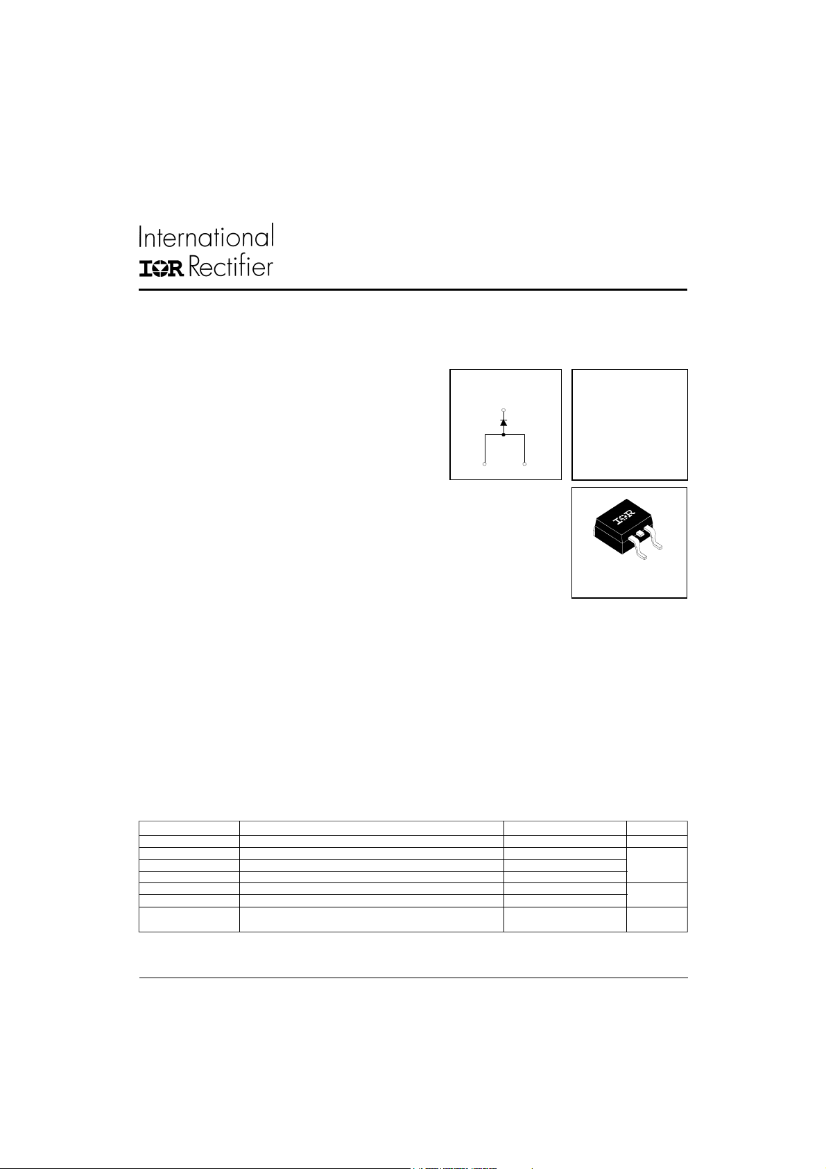
HFA06TB120S.. Series
Ultrafast, Soft Recovery DiodeHEXFRED
(N/C)
1
(K)
BASE
+
2
3
(A)
_
VR = 1200V
VF(typ.)* = 2.4V
I
F(AV)
Qrr (typ.)= 116nC
I
(typ.) = 4.4A
RRM
trr(typ.) = 26ns
di
/dt (typ.)* = 100A/µs
(rec)M
= 6.0A
Description
International Rectifier's HFA06TB120S is a state of the art ultra fast recovery diode.
Employing the latest in epitaxial construction and advanced processing techniques it
features a superb combination of characteristics which result in performance which is
unsurpassed by any rectifier previously available. With basic ratings of 1200 volts and 6
amps continuous current, the HFA06TB120S is especially well suited for use as the
companion diode for IGBTs and MOSFETs. In addition to ultra fast recovery time, the
HEXFRED product line features extremely low values of peak recovery current (I
does not exhibit any tendency to "snap-off" during the tb portion of recovery. The
RRM
) and
HEXFRED features combine to offer designers a rectifier with lower noise and significantly
lower switching losses in both the diode and the switching transistor. These HEXFRED
advantages can help to significantly reduce snubbing, component count and heatsink
sizes. The HEXFRED HFA06TB120S is ideally suited for applications in power supplies
and power conversion systems (such as inverters), motor drives, and many other similar
applications where high speed, high efficiency is needed.
Absolute Maximum Ratings
V
R
IF @ TC = 100°C Continuous Forward Current 8.0
I
FSM
I
FRM
PD @ TC = 25°C Maximum Power Dissipation 62.5
PD @ TC = 100°C Maximum Power Dissipation 25
T
J
T
STG
* 125°C
Parameter Max . Units
Cathode-to-Anode Voltage 1200 V
Single Pulse Forward Current 80 A
Maximum Repetitive Forward Current 24
Operating Junction and
Storage Temperature Range
-55 to +150
D2 Pak
W
°C
1
HFA06TB120S..Series
Bulletin PD-20602 rev. C 12/00
Electrical Characteristics @ TJ = 25°C (unless otherwise specified)
Parameter Min. Typ. Max. Units Test Conditions
V
V
I
RM
C
L
S
Dynamic Recovery Characteristics @ TJ = 25°C (unless otherwise specified)
Cathode Anode Breakdown 1200 ––– ––– V IR = 100µA
BR
Voltage
Max. Forward Voltage ––– 2.7 3.0 IF = 6.0A
FM
––– 3.5 3.9 V IF = 12A
––– 2.4 2.8 IF = 6.0A, TJ = 125°C
Max. Reverse Leakage Current ––– 0.26 5.0 VR = VR Rated
––– 110 500 TJ = 125°C, VR = 0.8 x VR Rated
Junction Capacitance ––– 9.0 14 pF VR = 200V
T
µA
Rated
Series Inductance ––– 8.0 ––– nH Measured lead to lead 5mm from pkg body
Parameter Min. Typ. Max. Units Test Conditions
D R
t
rr
t
rr1
t
rr2
I
RRM1
I
RRM2
Q
rr1
Q
rr2
di
(rec)M
di
(rec)M
Reverse Recovery Time ––– 26 ––– IF = 1.0A, dif/dt = 200A/µs, VR = 30V
––– 53 80 ns TJ = 25°C
––– 87 130 TJ = 125°C IF = 6.0A
Peak Recovery Current ––– 4.4 8.0 TJ = 25°C
A
––– 5.0 9.0 TJ = 125°C VR = 200V
Reverse Recovery Charge ––– 116 320 TJ = 25°C
––– 233 585 TJ = 125°C dif/dt = 200A/µs
nC
/dt1 Peak Rate of Recovery ––– 180 ––– TJ = 25°C
/dt2 Current During t
b
––– 100 ––– TJ = 125°C
A/µs
Thermal - Mechanical Characteristics
Parameter Min. Typ. Max. Units
T
lead
R
thJC
R
thJA
R
thCS
Wt Weight –––– 2.0 –––– g
! 0.063 in. from Case (1.6mm) for 10 sec
"#Typical Socket Mount
Lead Temperature –––– –––– 300 °C
!
Thermal Resistance, Junction to Case –––– –––– 2.0
Thermal Resistance, Junction to Ambient –––– –––– 80 K/ W
"
Thermal Resistance, Case to Heat Sink –––– 0.5 ––––
$
–––– 0.07 –––– (oz)
2
HFA06TB120S ..Series
0
Bulletin PD-20602 rev. C 12/00
100
10
(A)
F
1
Instantaneous Forward Current - I
T = 150˚C
J
T = 125˚C
J
T = 25˚C
J
1000
T = 150˚C
100
(µA)
R
10
J
125˚C
100˚C
1
25˚C
Reverse Current - I
0.1
0.01
0 200 400 600 800 1000 1200 1400
Reverse Voltage - VR (V)
100
(pF)
T
T = 25˚C
J
10
0.1
0246
Forward Voltage Drop - VFM (V)
Fig. 1 - Typical Forward Voltage Drop Characteristics
10
D = 0.50
D = 0.20
1
0.1
D = 0.10
D = 0.05
D = 0.02
D = 0.01
Single Pulse
thJC (°C/W)
(Thermal Resistance)
Thermal Impedance Z
.01
0.00001 0.0001 0.001 0.01 0.1 1 10 100
Fig. 4 - Maximum Thermal Impedance ZthJC Characteristics
Junction Capacitance - C
1
1 10 100 1000 10000
Reverse Voltage - VR (V)
Fig. 3 - Typical Junction Capacitance
Vs. Reverse Voltage
P
DM
t
1
t
2
Notes:
1. Duty factor D = t / t
2. Peak T = P x Z + T
1
2
J
DM
thJC
C
3

HFA06TB120S..Series
1
1
2
2
Bulletin PD-20602 rev. C 12/00
110
100
90
80
70
60
trr - ( nC )
50
40
V = 200V
R
T = 125˚C
J
T = 25˚C
30
J
20
100 1000
di
/dt - (A/µs )
f
Fig. 5 - Typical Reverse Recovery
Vs. di
/dt
f
1000
V = 200V
R
T = 125˚C
J
T = 25˚C
J
800
IF = 6 A
I
F
= 4 A
600
IF = 6 A
I
F
= 4 A
5
V = 200V
R
T = 125˚C
0
J
T = 25˚C
J
IF = 6 A
I
F
5
= 4 A
Irr - ( A)
0
5
0
100 1000
di
/dt - (A/µs )
f
Fig. 6 - Typical Recovery Current
Vs. di
/dt
f
10000
IF = 6 A
I
F
1000
= 4 A
M/dt - (A/µs )
Qrr - ( nC )
400
200
0
100 1000
di
/dt - (A/µs )
f
Fig. 8 - Typical Stored Charge vs. di
/dt
f
(REC)
100
di
10
100 1000
Fig. 7 - Typical di
V = 200V
T = 125˚C
T = 25˚C
di
/dt - (A/µs )
f
(REC)
R
J
J
M/dt vs. di
/dt
f
4
REVERSE RECOVERY CIRCUIT
V = 200V
R
0.01
Ω
L = 70µH
D.U.T.
HFA06TB120S ..Series
Bulletin PD-20602 rev. C 12/00
dif/dt
ADJUST
G
D
IRFP250
S
Fig. 9- Reverse Recovery Parameter Test Circuit
3
t
I
F
0
1
di /dt
f
rr
t
a
2
I
RRM
t
0.75
b
0.5
di(rec)M/dt
I
RRM
4
Q
rr
I
RRM
5
1. dif/dt - Rate of change of
current through zero
crossing
2. I
- Peak reverse
RRM
recovery current
3. trr - Reverse recovery
time measured from zero
crossing point of negative
going IF to point where a line
passing through 0.75 I
and 0.50 I
RRM
extrapolated to zero current
RRM
4. Qrr - Area under curve
defined by trr and I
t
Qrr =
2
5. di
(rec)M
change of current during t
portion of t
RRM
X I
rr
RRM
/dt - Peak rate of
rr
b
Fig. 10 - Reverse Recovery Waveform and Definitions
5

HFA06TB120S..Series
Bulletin PD-20602 rev. C 12/00
Outline Table
15.49 (0.61)
14.73 (0.58)
3X
Part Marking Information
93°
1.40 (0.055)
1.14 (0.045)
10.16 (0.40)
REF.
6.47 (0.25)
6.18 (0.24)
2.61 (0.10)
2.32 (0.09)
8.89 (0.35)
REF.
0.93 (0.37)
2X
0.69 (0.27)
13
2
4.57 (0.18)
4.32 (0.17)
0.61 (0.02) MAX.
5.08 (0.20) REF.
Conforms to JEDEC Outline D2PAK
Dimensions in millimeters and inches
4.69 (0.18)
4.20 (0.16)
1.32 (0.05)
1.22 (0.05)
5.28 (0.21)
4.78 (0.19)
0.55 (0.02)
0.46 (0.02)
MINIMU M REC OMMEND ED F OOTPRIN T
8.89 (0.35)
3.81 (0.15)
2.08 (0.08)
2X
11.43 (0.45)
17.78 (0.70)
2.54 (0.10)
2X
EXAMPLE: THIS IS AN HFA06TB120S
6
INTERNATIONAL
RECTIFIER LOGO
ASSEMBLY
LOT CODE
(K)
HFA06TB120S
5K3A
9712
(N/C) (A)
PART NUMBER
DATE CODE (YYWW)
YY = YEAR
WW = WEEK

Tape & Reel Information
HFA06TB120S ..Series
Bulletin PD-20602 rev. C 12/00
TRR
FEED DIRECTION
TRL
FEED DIRECTION
360 (14.173)
DIA. MAX.
13.50 (0.532)
12.80 (0.504)
1.85 (0.073)
1.65 (0.065)
DIA.
Ordering Information Table
4.10 (0.161)
3.90 (0.153)
10.90 (0.429 )
10.70 (0.421 )
1.60 (0.063)
1.50 (0.059)
1.60 (0.0 63)
1.50 (0.0 59)
11.60 (0.457)
11.40 (0.449)
1.75 (0 .069)
1.25 (0 .049)
16.10 ( 0.634)
15.90 ( 0.626)
26.40 ( 1.039)
24.40 ( 0.961)
60 (2.3 62)
DIA. MIN.
DIA.
15.42 ( 0.609)
15.22 ( 0.601)
DIA.
SMD-220 Tape & Reel
When orderi ng, indicate the par t
number, part orientation, and the
quant ity. Quanti ties are in mult iples
of 800 piece s per reel for both
TRL and T RR.
0.368 (0.0145)
0.342 (0.0135)
24.30 (0.957)
23.90 (0.941)
4.72 (0.186)
4.52 (0.178)
Device Code
HF A 06 TB 120 S TR
24
1
1 - Hexfred Family
2 - Process Designator
A = A subs. elec. irrad.
B = B subs. Platinum
3 - Average Current: Code 06 = 6 AMPS
4 - Package Outline: Code TB = TO-220 2 Lead
5 - Voltage code : Code 120 = 1200 V
6 - Configuration : Code S = SMD
7 - Suffix : Code TR = Tape and Reel
3
5
6
7
7

HFA06TB120S..Series
Bulletin PD-20602 rev. C 12/00
WORLD HEADQUARTERS: 233 Kansas St., El Segundo, California 90245 U.S.A. Tel: (310) 322 3331. Fax: (310) 322 3332.
EUROPEAN HEADQUARTERS: Hurst Green, Oxted, Surrey RH8 9BB, U.K. Tel: ++ 44 1883 732020. Fax: ++ 44 1883 733408.
IR SOUTHEAST ASIA: 1 Kim Seng Promenade, Great World City West Tower,13-11, Singapore 237994. Tel: ++ 65 838 4630.
8
IR CANADA: 15 Lincoln Court, Brampton, Markham, Ontario L6T3Z2. Tel: (905) 453 2200. Fax: (905) 475 8801.
IR GERMANY: Saalburgstrasse 157, 61350 Bad Homburg. Tel: ++ 49 6172 96590. Fax: ++ 49 6172 965933.
IR ITALY: Via Liguria 49, 10071 Borgaro, Torino. Tel: ++ 39 11 4510111. Fax: ++ 39 11 4510220.
IR FAR EAST: K&H Bldg., 2F, 30-4 Nishi-Ikebukuro 3-Chome, Toshima-Ku, Tokyo, Japan 171. Tel: 81 3 3983 0086.
IR TAIWAN: 16 Fl. Suite D.207, Sec. 2, Tun Haw South Road, Taipei, 10673, Taiwan. Tel: 886 2 2377 9936.
 Loading...