

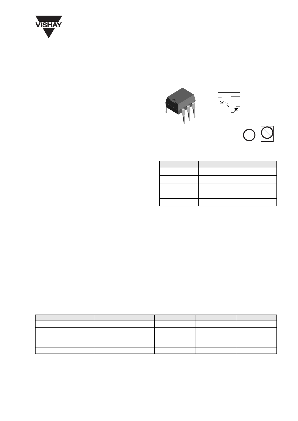
H11C4/ H11C5/ H11C6
1
2
3
6
5
4
G
A
C
A
C
NC
i179006
Vishay Semiconductors
Optocoupler, PhotoSCR Output, 400 V VRM, 5 A surge current
Features
• Turn on current (IFT), 5.0 mA typical
• Gate trigger current (I
• Surge anode current, 5.0 A
• Blocking voltage, 400 V gate trigger voltage (V
0.6 V typical
• Isolation test voltage 5300 V
• Solid State reliability
• Lead-free component
• Component in accordance to RoHS 2002/95/EC
and WEEE 2002/96/EC
), 20 mA typical
GT
RMS
GT
),
e3
Pb
Pb-free
Agency Approvals
• UL1577, File No. E52744 System Code H or J,
Double Protection
Description
The H11C4/ H11C5/ H11C6 are optically coupled
SCRs with a gallium arsenide infrared emitter and a
silicon photo SCR sensor. Switching can be achieved
while maintaining a high degree of isolation between
triggering and load circuits. These optocouplers can
Order Information
Part Remarks
H11C4 I
H11C5 I
H11C6 I
H11C4-X006 I
H11C6-X009 I
For additional information on the available options refer to
Option Information.
≤ 11 mA, DIP-6
FT
≤ 11 mA, DIP-6
FT
≤ 14 mA, DIP-6
FT
≤ 11 mA, DIP-6 400 mil (option 6)
FT
≤ 14 mA, SMD-6 (option 9)
FT
be used in SCR triac and solid state relay applications
where high blocking voltages and low input current
sensitivity are required.
The H11C4 and H11C5 are identical and have a maximum turn-on-current of 11 mA. The H11C6 has a
maximum of 14 mA.
Absolute Maximum Ratings
T
= 25 °C, unless otherwise specified
amb
Stresses in excess of the absolute Maximum Ratings can cause permanent damage to the device. Functional operation of the device is
not implied at these or any other conditions in excess of those given in the operational sections of this document. Exposure to absolute
Maximum Rating for extended periods of the time can adversely affect reliability.
Input
Parameter Test condition Symbol Val ue Unit
Peak reverse voltage V
Forward continuous current I
Peak forward current 1.0 ms, 1 % Duty Cycle I
Power dissipation P
Derate linearly from 25 °C 1.33 mW/°C
Document Number 83610
Rev. 1.6, 26-Oct-04
RM
F
FM
diss
6.0 V
60 mA
3.0 A
100 mW
www.vishay.com
1
H11C4/ H11C5/ H11C6
Vishay Semiconductors
Output
Parame te r Test condition Symbol Value Unit
Reverse gate voltage V
Anode voltage DC or AC peak V
RMS forward current I
Surge anode current 10 ms duration I
Peak forward current 100 µs, 1% Duty Cycle I
Surge gate current 5.0 ms duration I
Power dissipation P
RG
A
FRMS
AS
FM
GS
diss
Derate linearly from 25°C 13.3 mW/°C
Coupler
Parame te r Test condition Symbol Value Unit
Isolation test voltage (between
emitter and detector referred to
standard climate 23 °C/ 50 %
RH, DIN 50014)
Creepage ≥ 7.0 mm
Clearance ≥ 7.0 mm
Comparative tracking index per
DIN IEC 112/VDE 0303, part 1
Isolation resistance V
= 500 V, T
IO
V
= 500 V, T
IO
= 25 °C R
amb
= 100 °C R
amb
Total package dissipation P
Derate linearly from 25 °C 5.5 mW/°C
Operating temperature range T
Storage temperature range T
Lead soldering time at 260 °C 10 sec.
V
ISO
IO
IO
tot
amb
stg
6.0 V
400 V
300 mA
5.0 A
10 A
200 mA
1000 mW
5300 V
RMS
175
12
≥ 10
11
≥ 10
400 mW
- 55 to + 100 °C
- 55 to + 150 °C
Ω
Ω
Electrical Characteristics
T
= 25 °C, unless otherwise specified
amb
Minimum and maximum values are testing requirements. Typical values are characteristics of the device and are the result of engineering
evaluation. Typical values are for information only and are not part of the testing requirements.
Input
Parame te r Test condition Symbol Min Ty p. Max Unit
Forward voltage I
Reverse current V
Capacitance V
= 10 mA V
F
= 3.0 V I
R
= 0, f = 1.0 MHz C
R
F
R
O
1.2 1.5 V
10 µA
50 pF
Output
Parame te r Test condition Symbol Min Ty p. Max Unit
Forward blocking voltage R
Reverse blocking voltage R
On-state voltage I
Holding current R
www.vishay.com
2
= 10 KΩ, TA = 100 °C,
GK
= 150 µA
I
d
= 10 KΩ, TA = 100 °C,
GK
I
= 150 µA
d
= 300 mA V
T
= 27 KΩ, VFX = 50 V I
GK
V
DM
V
DM
t
H
400 V
400 V
1.1 1.3 V
500 µA
Document Number 83610
Rev. 1.6, 26-Oct-04

H11C4/ H11C5/ H11C6
Vishay Semiconductors
Parameter Test condition Symbol Min Ty p . Max Unit
Gate trigger voltage VFX = 100 V, RGK = 27 kΩ,
=10 KΩ
R
L
Forward leakage current R
Reverse leakage current R
Gate trigger current V
Capacitance, Anode to gate V = 0, f = 1.0 MHz 20 pF
Capacitance, Gate to cathode V = 0, f = 1.0 MHz 350 pF
= 10 KΩ, VRX = 400 V,
GK
= 0, TA = 100 °C
I
F
= 10 KΩ, VRX = 400 V,
GK
= 0, TA=100 °C
I
F
= 100 V, RRG = 27 KΩ,
FX
= 10 KΩ
R
L
Coupler
Parameter Test condition Part Symbol Min Ty p. Max Unit
Turn-on current V
= 50 V, RGK = 10 KΩ H11C4 I
DM
V
= 100 V, RGK = 27 KΩ H11C4 I
DM
V
GT
I
R
I
R
I
GT
H11C5 I
H11C6 I
H11C5 I
H11C6 I
0.6 1.0 V
150 µA
150 µA
20 50 µA
FT
FT
FT
FT
FT
FT
5.0 11 mA
5.0 11 mA
7.0 14 mA
20 mA
20 mA
30 mA
Package Dimensions in Inches (mm)
pin one ID
.130 (3.30)
.150 (3.81)
.031 (0.80) min.
.031 (0.80)
.035 (0.90)
.100 (2.54) typ.
.248 (6.30)
.256 (6.50)
.039
(1.00)
Min.
4°
typ.
.018 (0.45)
.022 (0.55)
i178004
3
4
5
.335 (8.50)
.343 (8.70)
12
6
.048 (0.45)
.022 (0.55)
3°–9°
ISO Method A
.300 (7.62)
typ.
18°
.010 (.25)
typ.
.300–.347
(7.62–8.81)
.114 (2.90)
.130 (3.0)
Document Number 83610
Rev. 1.6, 26-Oct-04
www.vishay.com
3

H11C4/ H11C5/ H11C6
Vishay Semiconductors
18493
Option 6
.407 (10.36)
.391 (9.96)
.307 (7.8)
.291 (7.4)
.014 (0.35)
.010 (0.25)
.400 (10.16)
.430 (10.92)
.0040 (.102)
.0098 (.249)
Option 9
.375 (9.53)
.395 (10.03)
.300 (7.62)
ref.
.020 (.51)
.040 (1.02)
.315 (8.00)
min.
.012 (.30) typ.
15° max.
www.vishay.com
4
Document Number 83610
Rev. 1.6, 26-Oct-04

H11C4/ H11C5/ H11C6
Vishay Semiconductors
Ozone Depleting Substances Policy Statement
It is the policy of Vishay Semiconductor GmbH to
1. Meet all present and future national and international statutory requirements.
2. Regularly and continuously improve the performance of our products, processes, distribution and
operatingsystems with respect to their impact on the health and safety of our employees and the public, as
well as their impact on the environment.
It is particular concern to control or eliminate releases of those substances into the atmosphere which are
known as ozone depleting substances (ODSs).
The Montreal Protocol (1987) and its London Amendments (1990) intend to severely restrict the use of ODSs
and forbid their use within the next ten years. Various national and international initiatives are pressing for an
earlier ban on these substances.
Vishay Semiconductor GmbH has been able to use its policy of continuous improvements to eliminate the use
of ODSs listed in the following documents.
1. Annex A, B and list of transitional substances of the Montreal Protocol and the London Amendments
respectively
2. Class I and II ozone depleting substances in the Clean Air Act Amendments of 1990 by the Environmental
Protection Agency (EPA) in the USA
3. Council Decision 88/540/EEC and 91/690/EEC Annex A, B and C (transitional substances) respectively.
Vishay Semiconductor GmbH can certify that our semiconductors are not manufactured with ozone depleting
substances and do not contain such substances.
We reserve the right to make changes to improve technical design
and may do so without further notice.
Parameters can vary in different applications. All operating parameters must be validated for each
customer application by the customer. Should the buyer use Vishay Semiconductors products for any
unintended or unauthorized application, the buyer shall indemnify Vishay Semiconductors against all
claims, costs, damages, and expenses, arising out of, directly or indirectly, any claim of personal
damage, injury or death associated with such unintended or unauthorized use.
Vishay Semiconductor GmbH, P.O.B. 3535, D-74025 Heilbronn, Germany
Telephone: 49 (0)7131 67 2831, Fax number: 49 (0)7131 67 2423
Document Number 83610
Rev. 1.6, 26-Oct-04
www.vishay.com
5

Legal Disclaimer Notice
Vishay
Document Number: 91000 www.vishay.com
Revision: 08-Apr-05 1
Notice
Specifications of the products displayed herein are subject to change without notice. Vishay Intertechnology, Inc.,
or anyone on its behalf, assumes no responsibility or liability for any errors or inaccuracies.
Information contained herein is intended to provide a product description only. No license, express or implied, by
estoppel or otherwise, to any intellectual property rights is granted by this document. Except as provided in Vishay's
terms and conditions of sale for such products, Vishay assumes no liability whatsoever, and disclaims any express
or implied warranty, relating to sale and/or use of Vishay products including liability or warranties relating to fitness
for a particular purpose, merchantability, or infringement of any patent, copyright, or other intellectual property right.
The products shown herein are not designed for use in medical, life-saving, or life-sustaining applications.
Customers using or selling these products for use in such applications do so at their own risk and agree to fully
indemnify Vishay for any damages resulting from such improper use or sale.
 Loading...