

GSOT03C-HT3 to GSOT36C-HT3
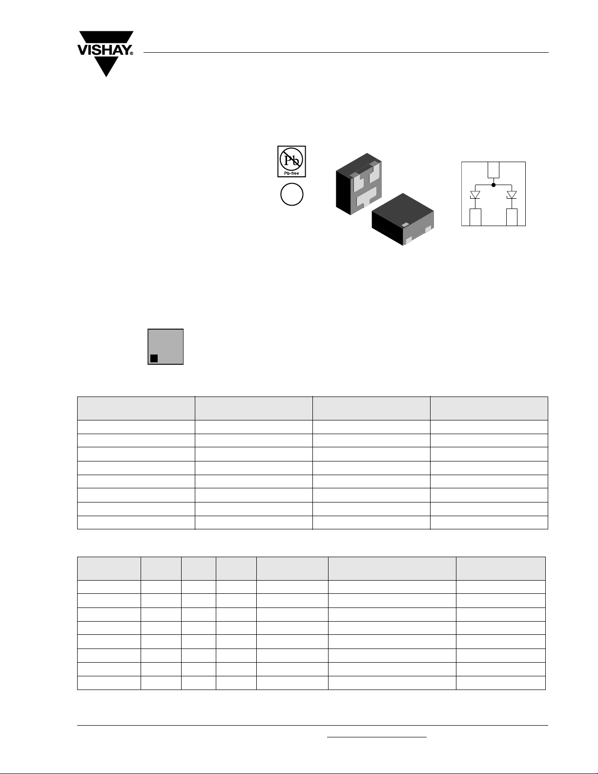
Two-Line ESD-Protection in LLP75
Features
• Two-line ESD-protection device
• ESD-immunity acc. IEC 61000-4-2
± 30 kV contact discharge
± 30 kV air discharge
• Space saving LLP package
• Lead (Pb)-free component
• Lead finish = "e3" = matte tin (Sn)
• Non-magnetic
• "Green" molding compound
• Component in accordance to RoHS 2002/95/EC
and WEEE 2002/96/EC
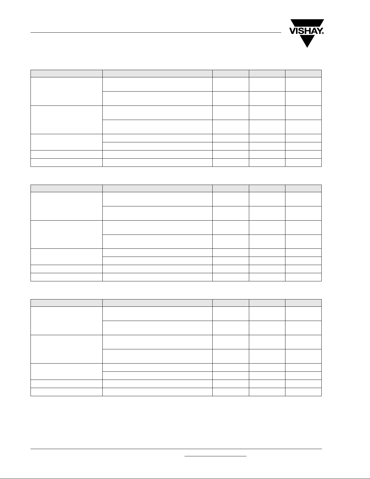
Marking (example only)
e3
20514
Vishay Semiconductors
3
1
1
2
20237
XX
Dot = Pin 1 marking
XX = Date code
YY
21001
YY = Type code (see table below)
Ordering Information
Device name Ordering code
GSOT03C-HT3 GSOT03C-HT3-GS08 3000 15000
GSOT04C-HT3 GSOT04C-HT3-GS08 3000 15000
GSOT05C-HT3 GSOT05C-HT3-GS08 3000 15000
GSOT08C-HT3 GSOT08C-HT3-GS08 3000 15000
GSOT12C-HT3 GSOT12C-HT3-GS08 3000 15000
GSOT15C-HT3 GSOT15C-HT3-GS08 3000 15000
GSOT24C-HT3 GSOT24C-HT3-GS08 3000 15000
GSOT36C-HT3 GSOT36C-HT3-GS08 3000 15000
Taped units per reel
(8 mm tape on 7" reel)
Minimum order quantity
Package Data
Device name
GSOT03C-HT3 LLP75-3B 03 5.1 mg UL 94 V-0 MSL level 1 (according J-STD-020) 260 °C/10 s at terminals
GSOT04C-HT3 LLP75-3B 04 5.1 mg UL 94 V-0 MSL level 1 (according J-STD-020) 260 °C/10 s at terminals
GSOT05C-HT3 LLP75-3B 05 5.1 mg UL 94 V-0 MSL level 1 (according J-STD-020) 260 °C/10 s at terminals
GSOT08C-HT3 LLP75-3B 08 5.1 mg UL 94 V-0 MSL level 1 (according J-STD-020) 260 °C/10 s at terminals
GSOT12C-HT3 LLP75-3B 12 5.1 mg UL 94 V-0 MSL level 1 (according J-STD-020) 260 °C/10 s at terminals
GSOT15C-HT3 LLP75-3B 15 5.1 mg UL 94 V-0 MSL level 1 (according J-STD-020) 260 °C/10 s at terminals
GSOT24C-HT3 LLP75-3B 24 5.1 mg UL 94 V-0 MSL level 1 (according J-STD-020) 260 °C/10 s at terminals
GSOT36C-HT3 LLP75-3B 36 5.1 mg UL 94 V-0 MSL level 1 (according J-STD-020) 260 °C/10 s at terminals
Package
name
Marking
code
Weight
Molding compound
flammability rating
Moisture sensitivity level Soldering conditions
Document Number 85825
Rev. 1.7, 21-Apr-08
For technical support, please contact: ESD-Protection@vishay.com
www.vishay.com
1
GSOT03C-HT3 to GSOT36C-HT3
Vishay Semiconductors
Absolute Maximum Ratings
GSOT03C-HT3
Rating Test con d iti o n Symbol Val ue Unit
Pin 1 to 3 or pin 2 to 3
Peak pulse current
Acc. IEC 61000-4-5, t
Pin 1 to 2 or pin 2 to 1; pin 3 not connected
Acc. IEC 61000-4-5, t
Pin 1 to 3 or pin 2 to 3
Peak pulse power
Acc. IEC 61000-4-5, t
Pin 1 to 2 or pin 2 to 1; pin 3 not connected
Acc. IEC 61000-4-5, t
ESD immunity
Contact discharge acc. IEC 61000-4-2; 10 pulses
Air discharge acc. IEC 61000-4-2; 10 pulses
Operating temperature Junction temperature
Storage temperature
GSOT04C-HT3
Rating Test con d iti o n Symbol Val ue Unit
Pin 1 to 3 or pin 2 to 3
Peak pulse current
Peak pulse power
ESD immunity
Operating temperature Junction temperature
Storage temperature
Acc. IEC 61000-4-5, t
Pin 1 to 2 or pin 2 to 1; pin 3 not connected
Acc. IEC 61000-4-5, t
Pin 1 to 3 or pin 2 to 3
Acc. IEC 61000-4-5, t
Pin 1 to 2 or pin 2 to 1; pin 3 not connected
Acc. IEC 61000-4-5, t
Contact discharge acc. IEC 61000-4-2; 10 pulses
Air discharge acc. IEC 61000-4-2; 10 pulses
= 8/20 µs; single shot
P
= 8/20 µs; single shot
P
= 8/20 µs; single shot
P
= 8/20 µs; single shot
P
= 8/20 µs; single shot
P
= 8/20 µs; single shot
P
= 8/20 µs; single shot
P
= 8/20 µs; single shot
P
I
I
P
P
V
V
T
I
I
P
P
V
V
T
PPM
PPM
PP
PP
ESD
ESD
T
STG
PPM
PPM
PP
PP
ESD
ESD
T
STG
30 A
30 A
369 W
504 W
± 30 kV
± 30 kV
J
- 40 to + 125 °C
- 55 to + 150 °C
30 A
30 A
429 W
564 W
± 30 kV
± 30 kV
J
- 40 to + 125 °C
- 55 to + 150 °C
GSOT05C-HT3
Rating Test con d iti o n Symbol Val ue Unit
Peak pulse current
Acc. IEC 61000-4-5, t
Pin 1 to 2 or pin 2 to 1; pin 3 not connected
Acc. IEC 61000-4-5, t
Peak pulse power
Acc. IEC 61000-4-5, t
Pin 1 to 2 or pin 2 to 1; pin 3 not connected
Acc. IEC 61000-4-5, t
ESD immunity
Contact discharge acc. IEC 61000-4-2; 10 pulses
Air discharge acc. IEC 61000-4-2; 10 pulses
Operating temperature Junction temperature
Storage temperature
www.vishay.com
For technical support, please contact: ESD-Protection@vishay.com
2
Pin 1 to 3 or pin 2 to 3
= 8/20 µs; single shot
P
= 8/20 µs; single shot
P
Pin 1 to 3 or pin 2 to 3
= 8/20 µs; single shot
P
= 8/20 µs; single shot
P
I
I
P
P
V
V
T
PPM
PPM
PP
PP
ESD
ESD
T
STG
30 A
30 A
480 W
612 W
± 30 kV
± 30 kV
J
- 40 to + 125 °C
- 55 to + 150 °C
Document Number 85825
Rev. 1.7, 21-Apr-08
GSOT03C-HT3 to GSOT36C-HT3
GSOT08C-HT3
Rating Test condition Symbol Val ue Unit
Peak pulse current
Acc. IEC 61000-4-5, t
Pin 1 to 2 or pin 2 to 1; pin 3 not connected
Acc. IEC 61000-4-5, t
Peak pulse power
Acc. IEC 61000-4-5, t
Pin 1 to 2 or pin 2 to 1; pin 3 not connected
Acc. IEC 61000-4-5, t
ESD immunity
Contact discharge acc. IEC 61000-4-2; 10 pulses
Air discharge acc. IEC 61000-4-2; 10 pulses
Operating temperature Junction temperature
Storage temperature
GSOT12C-HT3
Rating Test condition Symbol Val ue Unit
Peak pulse current
Peak pulse power
ESD immunity
Operating temperature Junction temperature
Storage temperature
Acc. IEC 61000-4-5, t
Pin 1 to 2 or pin 2 to 1; pin 3 not connected
Acc. IEC 61000-4-5, t
Acc. IEC 61000-4-5, t
Pin 1 to 2 or pin 2 to 1; pin 3 not connected
Acc. IEC 61000-4-5, t
Contact discharge acc. IEC 61000-4-2; 10 pulses
Air discharge acc. IEC 61000-4-2; 10 pulses
Pin 1 to 3 or pin 2 to 3
= 8/20 µs; single shot
P
= 8/20 µs; single shot
P
Pin 1 to 3 or pin 2 to 3
= 8/20 µs; single shot
P
= 8/20 µs; single shot
P
Pin 1 to 3 or pin 2 to 3
= 8/20 µs; single shot
P
= 8/20 µs; single shot
P
Pin 1 to 3 or pin 2 to 3
= 8/20 µs; single shot
P
= 8/20 µs; single shot
P
Vishay Semiconductors
I
I
P
P
V
V
T
I
I
P
P
V
V
T
PPM
PPM
PP
PP
ESD
ESD
T
STG
PPM
PPM
PP
PP
ESD
ESD
T
STG
J
J
18 A
18 A
345 W
400 W
± 30 kV
± 30 kV
- 40 to + 125 °C
- 55 to + 150 °C
12 A
12 A
312 W
337 W
± 30 kV
± 30 kV
- 40 to + 125 °C
- 55 to + 150 °C
GSOT15C-HT3
Rating Test condition Symbol Val ue Unit
Pin 1 to 3 or pin 2 to 3
Peak pulse current
Acc. IEC 61000-4-5, t
Pin 1 to 2 or pin 2 to 1; pin 3 not connected
Acc. IEC 61000-4-5, t
Pin 1 to 3 or pin 2 to 3
Peak pulse power
Acc. IEC 61000-4-5, t
Pin 1 to 2 or pin 2 to 1; pin 3 not connected
Acc. IEC 61000-4-5, t
ESD immunity
Contact discharge acc. IEC 61000-4-2; 10 pulses
Air discharge acc. IEC 61000-4-2; 10 pulses
Operating temperature Junction temperature
Storage temperature
= 8/20 µs; single shot
P
= 8/20 µs; single shot
P
= 8/20 µs; single shot
P
= 8/20 µs; single shot
P
I
I
P
P
V
V
T
PPM
PPM
PP
PP
ESD
ESD
T
STG
8A
8A
230 W
245 W
± 30 kV
± 30 kV
J
- 40 to + 125 °C
- 55 to + 150 °C
Document Number 85825
Rev. 1.7, 21-Apr-08
For technical support, please contact: ESD-Protection@vishay.com
www.vishay.com
3
GSOT03C-HT3 to GSOT36C-HT3
Vishay Semiconductors
GSOT24C-HT3
Rating Test con d iti o n Symbol Val ue Unit
Peak pulse current
Acc. IEC 61000-4-5, t
Pin 1 to 2 or pin 2 to 1; pin 3 not connected
Acc. IEC 61000-4-5, t
Peak pulse power
Acc. IEC 61000-4-5, t
Pin 1 to 2 or pin 2 to 1; pin 3 not connected
Acc. IEC 61000-4-5, t
ESD immunity
Contact discharge acc. IEC 61000-4-2; 10 pulses
Air discharge acc. IEC 61000-4-2; 10 pulses
Operating temperature Junction temperature
Storage temperature
GSOT36C-HT3
Rating Test con d iti o n Symbol Val ue Unit
Peak pulse current
Peak pulse power
ESD immunity
Operating temperature Junction temperature
Storage temperature
Acc. IEC 61000-4-5, t
Pin 1 to 2 or pin 2 to 1; pin 3 not connected
Acc. IEC 61000-4-5, t
Acc. IEC 61000-4-5, t
Pin 1 to 2 or pin 2 to 1; pin 3 not connected
Acc. IEC 61000-4-5, t
Contact discharge acc. IEC 61000-4-2; 10 pulses
Air discharge acc. IEC 61000-4-2; 10 pulses
Pin 1 to 3 or pin 2 to 3
= 8/20 µs; single shot
P
= 8/20 µs; single shot
P
Pin 1 to 3 or pin 2 to 3
= 8/20 µs; single shot
P
= 8/20 µs; single shot
P
Pin 1 to 3 or pin 2 to 3
= 8/20 µs; single shot
P
= 8/20 µs; single shot
P
Pin 1 to 3 or pin 2 to 3
= 8/20 µs; single shot
P
= 8/20 µs; single shot
P
I
I
P
P
V
V
T
I
I
P
P
V
V
T
PPM
PPM
PP
PP
ESD
ESD
T
STG
PPM
PPM
PP
PP
ESD
ESD
T
STG
5A
5A
235 W
240 W
± 30 kV
± 30 kV
J
- 40 to + 125 °C
- 55 to + 150 °C
3.5 A
3.5 A
248 W
252 W
± 30 kV
± 30 kV
J
- 40 to + 125 °C
- 55 to + 150 °C
www.vishay.com
4
For technical support, please contact: ESD-Protection@vishay.com
Document Number 85825
Rev. 1.7, 21-Apr-08

GSOT03C-HT3 to GSOT36C-HT3
Vishay Semiconductors
BiAs-Mode (2-line Bidirectional Asymmetrical protection mode)
With the GSOTxxC-HT3 two signal- or data-lines (L1, L2) can be protected against voltage transients. With
pin 3 connected to ground and pin 1 and pin 2 connected to a signal- or data-line which has to be protected.
As long as the voltage level on the data- or signal-line is between 0 V (ground level) and the specified Maximum
Reverse Working Voltage (V
offer a high isolation to the ground line. The protection device behaves like an open switch.
As soon as any positive transient voltage signal exceeds the break through voltage level of the protection
diode, the diode becomes conductive and shorts the transient current to ground. Now the protection device
behaves like a closed switch. The Clamping Voltage (V
plus the voltage drop at the series impedance (resistance and inductance) of the protection device.
Any negative transient signal will be clamped accordingly. The negative transient current is flowing in the
forward direction of the protection diode. The low Forward Voltage (V
the ground level.
Due to the different clamping levels in forward and reverse direction the GSOTxxC-HT3 clamping behaviour is
Bi
directional and Asymmetrical (BiAs).
L1
L2
) the protection diode between pin 2 and pin 3 and between pin 1 and pin 3
RWM
) is defined by the BReakthrough Voltage (VBR) level
C
) clamps the negative transient close to
F
1
2
3
If a higher surge current or Peak Pulse current (I
can also be used in parallel in order to "double" the performance.
) is needed, both protection diodes in the GSOTxxC-HT3
PP
This offers: • double surge power = double peak pulse current (2 x I
• halve line inductance = reduced clamping voltage
• halve line resistance = reduced clamping voltage
• double Diode Capacitance (2 x C
• double Reverse leakage current (2 x I
L1
1
2
3
)
D
)
R
20240
PPM
20239
)
Document Number 85825
Rev. 1.7, 21-Apr-08
For technical support, please contact: ESD-Protection@vishay.com
www.vishay.com
5

GSOT03C-HT3 to GSOT36C-HT3
Vishay Semiconductors
Electrical Characteristics
Ratings at 25 °C, ambient temperature unless otherwise specified
GSOT03C-HT3
BiAs mode (between pin 1 to 3 or pin 2 to 3)
Parameter Test conditions/remarks Symbol Min. Ty p. Max. Unit
Protection paths Number of lines which can be protected
= 100 µA V
Reverse stand off voltage
Reverse current
Reverse break down voltage
Reverse clamping voltage
Forward clamping voltage
Capacitance
at I
R
at V
= 3.3 V I
R
= 1 mA V
at I
R
= 1 A V
at I
PP
= I
at I
PP
at I
at I
PP
= 0 V; f = 1 MHz C
at V
R
at V
= 1.6 V; f = 1 MHz C
R
= 30 A V
PPM
= 1 A V
PP
= I
= 30 A V
PPM
GSOT04C-HT3
BiAs mode (between pin 1 to 3 or pin 2 to 3)
Parameter Test conditions/remarks Symbol Min. Ty p. Max. Unit
Protection paths Number of lines which can be protected
= 20 µA V
Reverse stand off voltage
Reverse current
Reverse break down voltage
Reverse clamping voltage
Forward clamping voltage
Capacitance
at I
R
= 4 V I
at V
R
= 1 mA V
at I
R
= 1 A V
at I
PP
= I
at I
PP
at I
at I
PP
= 0 V; f = 1 MHz C
at V
R
at V
= 2 V; f = 1 MHz C
R
= 30 A V
PPM
= 1 A V
PP
= I
= 30 A V
PPM
N
N
lines
RWM
R
BR
C
C
F
F
D
D
lines
RWM
R
BR
C
C
F
F
D
D
2 lines
3.3 V
100 µA
44.6 V
5.7 7.5 V
10 12.3 V
11.2V
4.5 V
420 600 pF
260 pF
2 lines
4V
20 µA
56.1 V
7.5 9 V
11.2 14.3 V
11.2V
4.5 V
310 450 pF
200 pF
GSOT05C-HT3
BiAs mode (between pin 1 to 3 or pin 2 to 3)
Parameter Test conditions/remarks Symbol Min. Ty p. Max. Unit
Protection paths Number of lines which can be protected
= 10 µA V
Reverse stand off voltage
Reverse current
Reverse break down voltage
Reverse clamping voltage
Forward clamping voltage
Capacitance
www.vishay.com
6
For technical support, please contact: ESD-Protection@vishay.com
at I
R
at V
= 5 V I
R
= 1 mA V
at I
R
at I
= 1 A V
PP
= I
at I
PP
at I
at I
PP
= 0 V; f = 1 MHz C
at V
R
= 2.5 V; f = 1 MHz C
at V
R
= 30 A V
PPM
= 1 A V
PP
= I
= 30 A V
PPM
N
lines
RWM
R
BR
C
C
F
F
D
D
2 lines
5V
10 µA
66.8 V
78.7V
12 16 V
11.2V
4.5 V
260 350 pF
150 pF
Document Number 85825
Rev. 1.7, 21-Apr-08

GSOT03C-HT3 to GSOT36C-HT3
GSOT08C-HT3
BiAs mode (between pin 1 to 3 or pin 2 to 3)
Parameter Test conditions/remarks Symbol Min. Ty p. Max. Unit
Protection paths Number of lines which can be protected
= 5 µA V
Reverse stand off voltage
Reverse current
Reverse break down voltage
Reverse clamping voltage
Forward clamping voltage
Capacitance
GSOT12C-HT3
BiAs mode (between pin 1 to 3 or pin 2 to 3)
Parameter Test conditions/remarks Symbol Min. Ty p. Max. Unit
Protection paths Number of lines which can be protected
Reverse stand off voltage
Reverse current
Reverse break down voltage
Reverse clamping voltage
Forward clamping voltage
Capacitance
at I
R
= 8 V I
at V
R
= 1 mA V
at I
R
= 1 A V
at I
PP
= I
at I
PP
at I
at I
PP
at V
= 0 V; f = 1 MHz C
R
= 4 V; f = 1 MHz C
at V
R
at I
at V
at I
at I
at I
PP
at I
at I
PP
= 0 V; f = 1 MHz C
at V
R
at V
= 6 V; f = 1 MHz C
R
= 18 A V
PPM
= 1 A V
PP
= I
= 18 A V
PPM
= 1 µA V
R
= 12 V I
R
= 1 mA V
R
= 1 A V
PP
= I
= 12 A V
PPM
= 1 A V
PP
= I
= 12 A V
PPM
N
N
lines
RWM
R
BR
C
C
F
F
D
D
lines
RWM
R
BR
C
C
F
F
D
D
Vishay Semiconductors
2 lines
8V
5µA
910 V
10.7 13 V
15.2 19.2 V
11.2V
3V
160 250 pF
80 pF
2 lines
12 V
1µA
13.5 15 V
15.4 18.7 V
21.2 26 V
11.2V
2.2 V
115 150 pF
50 pF
GSOT15C-HT3
BiAs mode (between pin 1 to 3 or pin 2 to 3)
Parameter Test conditions/remarks Symbol Min. Ty p. Max. Unit
Protection paths Number of lines which can be protected
at I
Reverse stand off voltage
Reverse current
Reverse break down voltage
Reverse clamping voltage
Forward clamping voltage
Capacitance
Document Number 85825
Rev. 1.7, 21-Apr-08
at V
at V
For technical support, please contact: ESD-Protection@vishay.com
= 1 µA V
R
= 15 V I
at V
R
= 1 mA V
at I
R
= 1 A V
at I
PP
= I
at I
PP
at I
at I
PP
= 0 V; f = 1 MHz C
R
= 7.5 V; f = 1 MHz C
R
= 8 A V
PPM
= 1 A V
PP
= I
= 8 A V
PPM
N
lines
RWM
R
BR
C
C
F
F
D
D
2 lines
15 V
1µA
16.5 18 V
19.4 23.5 V
24.8 28.8 V
11.2V
1.8 V
90 120 pF
35 pF
www.vishay.com
7

GSOT03C-HT3 to GSOT36C-HT3
Vishay Semiconductors
GSOT24C-HT3
BiAs mode (between pin 1 to 3 or pin 2 to 3)
Parameter Test conditions/remarks Symbol Min. Ty p. Max. Unit
Protection paths Number of lines which can be protected
= 1 µA V
Reverse stand off voltage
Reverse current
Reverse break down voltage
Reverse clamping voltage
Forward clamping voltage
Capacitance
at I
R
at V
= 24 V I
R
= 1 mA V
at I
R
= 1 A V
at I
PP
= I
at I
PP
at I
at I
PP
= 0 V; f = 1 MHz C
at V
R
at V
= 12 V; f = 1 MHz C
R
= 5 A V
PPM
= 1 A V
PP
= I
= 5 A V
PPM
GSOT36C-HT3
BiAs mode (between pin 1 to 3 or pin 2 to 3)
Parameter Test conditions/remarks Symbol Min. Ty p. Max. Unit
Protection paths Number of lines which can be protected
at I
Reverse stand off voltage
Reverse current
Reverse break down voltage
Reverse clamping voltage
Forward clamping voltage
Capacitance
at I
at I
at V
at V
= 1 µA V
R
= 36 V I
at V
R
at I
= 1 mA V
R
= 1 A V
at I
PP
= I
PP
PP
R
= 18 V; f = 1 MHz C
R
= 3.5 A V
PPM
= 1 A V
at I
PP
= I
= 3.5 A V
PPM
= 0 V; f = 1 MHz C
N
N
lines
RWM
R
BR
C
C
F
F
D
D
lines
RWM
R
BR
C
C
F
F
D
D
2 lines
24 V
1µA
27 30 V
34 41 V
41 47 V
11.2V
1.4 V
65 80 pF
20 pF
2 lines
36 V
1µA
39 43 V
49 60 V
59 71 V
11.2V
1.3 V
52 65 pF
12 pF
www.vishay.com
8
For technical support, please contact: ESD-Protection@vishay.com
Document Number 85825
Rev. 1.7, 21-Apr-08

GSOT03C-HT3 to GSOT36C-HT3
Vishay Semiconductors
BiSy-mode (1-line Bidirectional Symmetrical protection mode)
If a bipolar symmetrical protection device is needed the GSOTxxC-HT3 can also be used as a single line
protection device. Therefore pin 1 has to be connected to the signal- or data-line (L1) and pin 2 to ground
(or vice versa). pin 3 must not be connected.
Positive and negative voltage transients will be clamped in the same way. The clamping current through the
GSOTxxC-HS3 passes one diode in forward direction and the other one in reverse direction. The Clamping
Voltage (V
other diode plus the voltage drop at the series impedances (resistances and inductances) of the protection
device.
Due to the same clamping levels in positive and negative direction the GSOTxxC-HT3 voltage clamping
behaviour is Bi
) is defined by the BReakthrough Voltage (VBR) level of one diode plus the forward voltage of the
C
directional and Symmetrical (BiSy).
L1
1
3
2
Electrical Characteristics
Ratings at 25 °C, ambient temperature unless otherwise specified
GSOT03C-HT3
BiSy mode (between pin 1 to 2 or pin 2 to 1; pin 3 not connected)
Parameter Test conditions/remarks Symbol Min. Ty p. Max. Unit
Protection paths Number of lines which can be protected
at I
Reverse stand off voltage
Reverse current
Reverse break down voltage
Clamping voltage
Capacitance
at V
= 100 µA V
R
= 3.8 V I
at V
R
at I
= 1 mA V
R
= 1 A V
at I
PP
= I
at I
PP
= 0 V; f = 1 MHz C
at V
R
= 1.6 V; f = 1 MHz C
R
= 30 A V
PPM
N
lines
RWM
R
BR
C
C
D
D
GSOT04C-HT3
BiSy mode (between pin 1 to 2 or pin 2 to 1; pin 3 not connected)
Parameter Test conditions/remarks Symbol Min. Ty p. Max. Unit
Protection paths Number of lines which can be protected
= 20 µA V
Reverse stand off voltage
Reverse current
Reverse break down voltage
Clamping voltage
Capacitance
at I
R
at V
= 4.5 V I
R
= 1 mA V
at I
R
at I
= 1 A V
PP
= I
at I
PP
at V
= 0 V; f = 1 MHz C
R
= 2 V; f = 1 MHz C
at V
R
= 30 A V
PPM
N
lines
RWM
R
BR
C
C
D
D
20241
1 lines
3.8 V
100 µA
4.5 5.3 V
78.4V
14 16.8 V
210 300 pF
190 pF
1 lines
4.5 V
20 µA
5.5 6.8 V
7.5 9 V
15.7 18.8 V
155 225 pF
135 pF
Document Number 85825
Rev. 1.7, 21-Apr-08
For technical support, please contact: ESD-Protection@vishay.com
www.vishay.com
9

GSOT03C-HT3 to GSOT36C-HT3
Vishay Semiconductors
GSOT05C-HT3
BiSy mode (between pin 1 to 2 or pin 2 to 1; pin 3 not connected)
Parameter Test conditions/remarks Symbol Min. Ty p. Max. Unit
Protection paths Number of lines which can be protected
= 10 µA V
Reverse stand off voltage
Reverse current
Reverse break down voltage
Clamping voltage
Capacitance
at I
R
at V
= 5.5 V I
R
= 1 mA V
at I
R
= 1 A V
at I
PP
= I
at I
PP
= 0 V; f = 1 MHz C
at V
R
= 2.5 V; f = 1 MHz C
at V
R
= 30 A V
PPM
GSOT08C-HT3
BiSy mode (between pin 1 to 2 or pin 2 to 1; pin 3 not connected)
Parameter Test conditions/remarks Symbol Min. Ty p. Max. Unit
Protection paths Number of lines which can be protected
at I
Reverse stand off voltage
Reverse current
Reverse break down voltage
Clamping voltage
Capacitance
at I
at V
at V
= 5 µA V
R
= 8.5 V I
at V
R
at I
= 1 mA V
R
= 1 A V
at I
PP
= I
PP
= 0 V; f = 1 MHz C
R
= 4 V; f = 1 MHz C
R
= 18 A V
PPM
N
N
lines
RWM
R
BR
C
C
D
D
lines
RWM
R
BR
C
C
D
D
1 lines
5.5 V
10 µA
6.5 7.5 V
8.1 9.7 V
17 20.4 V
130 175 pF
100 pF
1 lines
8.5 V
5µA
9.5 10.7 V
11.7 14 V
18.5 22.2 V
80 125 pF
60 pF
GSOT12C-HT3
BiSy mode (between pin 1 to 2 or pin 2 to 1; pin 3 not connected)
Parameter Test conditions/remarks Symbol Min. Ty p. Max. Unit
Protection paths Number of lines which can be protected
= 1 µA V
Reverse stand off voltage
Reverse current
Reverse break down voltage
Clamping voltage
Capacitance
at I
R
= 12.5 V I
at V
R
= 1 mA V
at I
R
= 1 A V
at I
PP
= I
at I
PP
at V
= 0 V; f = 1 MHz C
R
= 6 V; f = 1 MHz C
at V
R
= 12 A V
PPM
GSOT15C-HT3
BiSy mode (between pin 1 to 2 or pin 2 to 1; pin 3 not connected)
Parameter Test conditions/remarks Symbol Min. Ty p. Max. Unit
Protection paths Number of lines which can be protected
= 1 µA V
Reverse stand off voltage
Reverse current
Reverse break down voltage
Clamping voltage
Capacitance
at I
R
= 15.5 V I
at V
R
= 1 mA V
at I
R
= 1 A V
at I
PP
= I
at I
PP
= 0 V; f = 1 MHz C
at V
R
= 7.5 V; f = 1 MHz C
at V
R
= 8 A V
PPM
N
N
lines
RWM
R
BR
C
C
D
D
lines
RWM
R
BR
C
C
D
D
1 lines
12.5 V
1µA
13.5 15.7 V
16.4 19.7 V
23.4 28.1 V
58 75 pF
36 pF
1 lines
15.5 V
1µA
17 18.7 V
20.4 24.5 V
26.6 30.6 V
45 60 pF
25 pF
www.vishay.com
10
For technical support, please contact: ESD-Protection@vishay.com
Document Number 85825
Rev. 1.7, 21-Apr-08

GSOT03C-HT3 to GSOT36C-HT3
GSOT24C-HT3
BiSy mode (between pin 1 to 2 or pin 2 to 1; pin 3 not connected)
Parameter Test conditions/remarks Symbol Min. Ty p. Max. Unit
Protection paths Number of lines which can be protected
= 1 µA V
Reverse stand off voltage
Reverse current
Reverse break down voltage
Clamping voltage
Capacitance
GSOT36C-HT3
BiSy mode (between pin 1 to 2 or pin 2 to 1; pin 3 not connected)
Parameter Test conditions/remarks Symbol Min. Ty p. Max. Unit
Protection paths Number of lines which can be protected
Reverse stand off voltage
Reverse current
Reverse break down voltage
Clamping voltage
Capacitance
at I
R
at V
= 24.5 V I
R
= 1 mA V
at I
R
= 1 A V
at I
PP
= I
at I
PP
= 0 V; f = 1 MHz C
at V
R
= 12 V; f = 1 MHz C
at V
R
at I
at V
at I
at I
at I
PP
= 0 V; f = 1 MHz C
at V
R
= 18 V; f = 1 MHz C
at V
R
= 5 A V
PPM
= 1 µA V
R
= 36.5 V I
R
= 1 mA V
R
= 1 A V
PP
= I
= 3.5 A V
PPM
N
N
lines
RWM
R
BR
C
C
D
D
lines
RWM
R
BR
C
C
D
D
Vishay Semiconductors
1 lines
24.5 V
1µA
27.5 30.7 V
34 41 V
40 48 V
33 40 pF
18 pF
1 lines
36.5 V
1µA
39.5 43.7 V
50 60 V
60 72 V
26 33 pF
10 pF
Package Dimensions in millimeters (inches): LLP75-3B
18057
Document Number 85825
Rev. 1.7, 21-Apr-08
For technical support, please contact: ESD-Protection@vishay.com
www.vishay.com
11

GSOT03C-HT3 to GSOT36C-HT3
Vishay Semiconductors
Ozone Depleting Substances Policy Statement
It is the policy of Vishay Semiconductor GmbH to
1. Meet all present and future national and international statutory requirements.
2. Regularly and continuously improve the performance of our products, processes, distribution and operating
systems with respect to their impact on the health and safety of our employees and the public, as well as
their impact on the environment.
It is particular concern to control or eliminate releases of those substances into the atmosphere which are
known as ozone depleting substances (ODSs).
The Montreal Protocol (1987) and its London Amendments (1990) intend to severely restrict the use of ODSs
and forbid their use within the next ten years. Various national and international initiatives are pressing for an
earlier ban on these substances.
Vishay Semiconductor GmbH has been able to use its policy of continuous improvements to eliminate the use
of ODSs listed in the following documents.
1. Annex A, B and list of transitional substances of the Montreal Protocol and the London Amendments
respectively.
2. Class I and II ozone depleting substances in the Clean Air Act Amendments of 1990 by the Environmental
Protection Agency (EPA) in the USA.
3. Council Decision 88/540/EEC and 91/690/EEC Annex A, B and C (transitional substances) respectively.
Vishay Semiconductor GmbH can certify that our semiconductors are not manufactured with ozone depleting
substances and do not contain such substances.
We reserve the right to make changes to improve technical design
and may do so without further notice.
Parameters can vary in different applications. All operating parameters must be validated for each customer
application by the customer. Should the buyer use Vishay Semiconductors products for any unintended or
unauthorized application, the buyer shall indemnify Vishay Semiconductors against all claims, costs, damages,
and expenses, arising out of, directly or indirectly, any claim of personal damage, injury or death associated
with such unintended or unauthorized use.
Vishay Semiconductor GmbH, P.O.B. 3535, D-74025 Heilbronn, Germany
www.vishay.com
12
For technical support, please contact: ESD-Protection@vishay.com
Document Number 85825
Rev. 1.7, 21-Apr-08

Legal Disclaimer Notice
Vishay
Notice
Specifications of the products displayed herein are subject to change without notice. Vishay Intertechnology, Inc.,
or anyone on its behalf, assumes no responsibility or liability for any errors or inaccuracies.
Information contained herein is intended to provide a product description only. No license, express or implied, by
estoppel or otherwise, to any intellectual property rights is granted by this document. Except as provided in Vishay's
terms and conditions of sale for such products, Vishay assumes no liability whatsoever, and disclaims any express
or implied warranty, relating to sale and/or use of Vishay products including liability or warranties relating to fitness
for a particular purpose, merchantability, or infringement of any patent, copyright, or other intellectual property right.
The products shown herein are not designed for use in medical, life-saving, or life-sustaining applications.
Customers using or selling these products for use in such applications do so at their own risk and agree to fully
indemnify Vishay for any damages resulting from such improper use or sale.
Document Number: 91000 www.vishay.com
Revision: 08-Apr-05 1
 Loading...