

Page 1
GBPC12, GBPC15, GBPC25 & GBPC35
Vishay General Semiconductor
Glass Passivated Single-Phase Bridge Rectifier
FEATURES
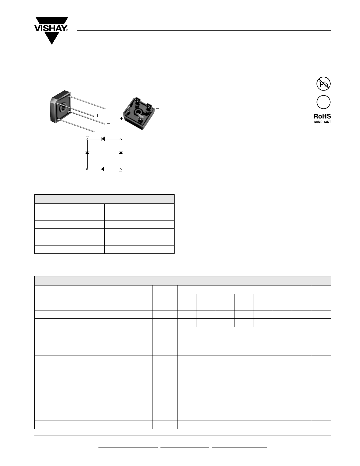
GBPCGBPC-W
~
~
~
~
~
~
• UL recognition file number E54214
• Universal 3-way terminals: snap-on, wire
wrap-around, or P.C.B. mounting
• Typical I
less than 0.3 µA
R
• High surge current capability
• Low thermal resistance
• Solder dip 260 °C, 40 s
• Component in accordance to RoHS 2002/95/EC
and WEEE 2002/96/EC
TYPICAL APPLICATIONS
General purpose use in ac-to-dc bridge full wave
rectification for power supply, home appliances, office
equipment, industrial automation applications.
e4
PRIMARY CHARACTERISTICS
I
F(AV)
V
RRM
I
FSM
I
R
V
F
T
max. 150 °C
J
12 A, 15 A, 25 A, 35 A
50 V to 1000 V
200 A, 300 A, 300 A, 400 A
5 µA
1.1 V
MECHANICAL DATA
Case: GBPC, GBPC-W
Epoxy meets UL 94V-0 flammability rating
Terminals: Nickel plated on faston lugs or silver
plated on wire leads, solderable per J-STD-002
and JESD22-B102. E4 suffix for consumer grade.
Suffix letter “W” added to indicate wire leads
(e.g. GBPC12005W).
Polarity: As marked, positive lead by belevled corner
Mounting Torque: 20 inches-lbs. max.
MAXIMUM RATINGS (TA = 25 °C unless otherwise noted)
PARAMETER SYMBOL
Maximum repetitive peak reverse voltage V
Maximum RMS voltage V
Maximum DC blocking voltage V
GBPC12
Maximum average forward rectified
output current (Fig. 1)
Peak forward surge current single
sine-wave superimposed on rated load
GBPC15
GBPC25
GBPC35
GBPC12
GBPC15
GBPC25
GBPC35
RRM
RMS
I
F(AV)
I
FSM
DC
005 01 02 04 06 08 10
50 100 200 400 600 800 1000 V
35 70 140 280 420 560 700 V
50 100 200 400 600 800 1000 V
GBPC12, 15, 25, 35
12
15
25
35
200
300
300
400
UNIT
A
A
GBPC12
Rating (non-repetitive, for t greater than
1 ms and less than 8.3 ms) for fusing
RMS isolation voltage from case to leads V
Operating junction storage temperature range T
Document Number: 88612
Revision: 15-Apr-08
For technical questions within your region, please contact one of the following:
PDD-Americas@vishay.com
GBPC15
GBPC25
GBPC35
160
2
I
t
2500 V
ISO
, T
J
STG
, PDD-Asia@vishay.com, PDD-Europe@vishay.com
375
375
660
- 55 to + 150 °C
www.vishay.com
A
2
s
1
Page 2
GBPC12, GBPC15, GBPC25 & GBPC35
Vishay General Semiconductor
ELECTRICAL CHARACTERISTICS (TA = 25 °C unless otherwise noted)
PARAMETER
GBPC12
Maximum instantaneous
forward drop per diode
Maximum reverse DC current at rated
DC blocking voltage per diode
Typical junction capacitance per diode 4 V, 1 MHz C
GBPC15
GBPC25
GBPC35
TEST
CONDITIONS
I
= 6.0 A
F
I
= 7.5 A
F
I
= 12.5 A
F
I
= 17.5 A
F
= 25 °C
T
A
T
= 125 °C
A
SYMBOL
V
F
I
R
005 01 02 04 06 08 10
300 pF
J
THERMAL CHARACTERISTICS (TA = 25 °C unless otherwise noted)
PARAMETER SYMBOL
Typical thermal resistance
Notes:
(1) With heatsink
(2) Bolt down on heatsink with silicone thermal compound between bridge and mounting surface for maximum heat transfer with #10 screw
(1)
GBPC12-25
GBPC35
R
θJC
005 01 02 04 06 08 10
GBPC12, 15, 25, 35
1.1 V
5.0
500
GBPC12, 15, 25, 35
1.9
1.4
UNIT
µA
UNIT
°C/W
ORDERING INFORMATION (Example)
PREFERRED P/N UNIT WEIGHT (g) PREFERRED PACKAGE CODE BASE QUANTITY DELIVERY MODE
GBPC1206-E4/51 15.79 51 100 Paper box
GBPC1506-E4/51 15.79 51 100 Paper box
GBPC2506-E4/51 15.79 51 100 Paper box
GBPC3506-E4/51 15.79 51 100 Paper box
GBPC1206W-E4/51 13.8 51 100 Paper box
GBPC1506W-E4/51 13.8 51 100 Paper box
GBPC2506W-E4/51 13.8 51 100 Paper box
GBPC3506W-E4/51 13.8 51 100 Paper box
www.vishay.com For technical questions within your region, please contact one of the following:
2
PDD-Americas@vishay.com
, PDD-Asia@vishay.com, PDD-Europe@vishay.com
Document Number: 88612
Revision: 15-Apr-08
Page 3

GBPC12, GBPC15, GBPC25 & GBPC35
C
RATINGS AND CHARACTERISTICS CURVES
(T
= 25 °C unless otherwise noted)
A
Vishay General Semiconductor
40
35
30
25
20
15
10
Average Forward Current (A)
5
0
60 Hz
Resistive or
Inductive Load
25
0
50
75
Bridges Mo
9.5 x 3.5 x 4.6"
(22.9 x 8.9 x 11.7 cm)
AL, Finned Plate
unte
5 x 6 x 4.9"
AL, Finned Plate
5 x 4 x 3"
AL, Finned Plate
100
125
Case Temperature (°C)
Figure 1. Maximum Output Rectified Current
40
GBPC35
R
= 0.5 °C/W
thSA
35
30
GBPC25
rrent (A)
R
= 0.5 °C/W
25
20
15
10
5
0
thSA
GBPC15
R
thSA
GBPC12
R
thSA
0
= 1.0 °C/W
= 1.0 °C/W
10
20
30
40
50
60
u
Average Forward
Ambient Temperature (°C)
Figure 2. Maximum Output Rectified Current
d on
6 x 2.2 x 2.2"
AL, Finned Plate
150
175
60 Hz
Resistive or
Inductive Load
70
80
90
200
100
1000
100
Peak Forward Surge Current (A)
10
1.0 Cycle
1
TJ = TJ Max.
0.5 ms Single Sine-Wave
GBPC35
GBPC12
GBPC15
GBPC25
10
100
Number of Cycles at 60 Hz
Figure 4. Maximum Non-Repetitive Peak Forward Surge
Current Per Diode
100
TA = 150 °C
T
= 125 °C
10
1
A
TA = 100 °C
TA = 25 °C
Instantaneous Forward Current (A)
0.1
0.4
0.5
0.6
0.7
0.8
0.9
1.0
1.1
Instantaneous Forward Voltage (V)
Figure 5. Typical Instantaneous Forward Characteristics Per Diode
80
70
60
50
40
30
20
10
Average Power Dissipation of Bridge (W)
0
0
Capacitive Load
TJ = TJ Max.
10
Average Output Current (A)
20
Resistive or
Inductive Load
30
40
Figure 3. Maximum Power Dissipation
1000
100
10
TA = 150 °C
T
= 125 °C
A
TA = 100 °C
Current (µA)
1
Instantaneous Reverse Leakage
0.1
0
20
10
TA = 25 °C
30
40
50
60
70
80
90
100
Percent of Rated Peak Reverse Voltage (%)
Figure 6. Typical Reverse Leakage Characteristics Per Diode
Document Number: 88612
Revision: 15-Apr-08
For technical questions within your region, please contact one of the following:
PDD-Americas@vishay.com
, PDD-Asia@vishay.com, PDD-Europe@vishay.com
www.vishay.com
3
Page 4

GBPC12, GBPC15, GBPC25 & GBPC35
Vishay General Semiconductor
1000
TJ = 25 °C
f = 1.0 MHz
= 50 mVp-p
V
sig
100
Junction Capacitance (pF)
10
1
10
100
Reverse Voltage (V)
Figure 7. Typical Junction Capacitance Per Diode
PACKAGE OUTLINE DIMENSIONS in inches (millimeters)
GBPC-W GBPC
Hole for
#10 Screw
0.220 (5.59)
0.200 (5.08)
DIA.
1.135 (28.8)
1.115 (28.3)
0.732 (18.6)
0.692 (17.6)
0.24 (6.0)
0.18 (4.6)
0.220 (5.59)
0.200 (5.08)
Transient Thermal Impedance (°C/W)
1000
100
10
1
0.01
0.1
1
TJ = 25 °C
f = 1.0 MHz
= 50 mVp-p
V
sig
10
100
t - Heating Time (s)
Figure 8. Typical Transient Thermal Impedance Per Diode
DIA.
1.135 (28.8)
1.115 (28.3)
0.672 (17.1)
0.632 (16.1)
AC
Hole for
#10 Screw
1.135 (28.8)
1.115 (28.3)
0.24 (6.0)
0.18 (4.6)
0.042 (1.07)
0.038 (0.97)
DIA.
0.310 (7.62)
0.290 (7.36)
0.470 (11.9)
0.430 (10.9)
0.732 (18.6)
0.692 (17.6)
0.50 (12.7)
0.44 (11.7)
1.25
(31.8)
MIN.
1.135 (28.8)
1.115 (28.3)
0.310 (7.62)
0.290 (7.36)
0.672 (17.1)
0.632 (16.1)
0.034 (0.86)
0.030 (0.76)
0.094 (2.4)
DIA.
0.034 (0.86)
0.030 (0.76)
0.732 (18.6)
0.692 (17.6)
0.25
(6.35)
0.582 (14.8)
0.542 (13.8)
0.840 (21.3)
0.740 (18.8)
www.vishay.com For technical questions within your region, please contact one of the following:
4
PDD-Americas@vishay.com
, PDD-Asia@vishay.com, PDD-Europe@vishay.com
Document Number: 88612
Revision: 15-Apr-08
Page 5

Legal Disclaimer Notice
Vishay
Disclaimer
All product specifications and data are subject to change without notice.
Vishay Intertechnology, Inc., its affiliates, agents, and employees, and all persons acting on its or their behalf
(collectively, “Vishay”), disclaim any and all liability for any errors, inaccuracies or incompleteness contained herein
or in any other disclosure relating to any product.
Vishay disclaims any and all liability arising out of the use or application of any product described herein or of any
information provided herein to the maximum extent permitted by law. The product specifications do not expand or
otherwise modify Vishay’s terms and conditions of purchase, including but not limited to the warranty expressed
therein, which apply to these products.
No license, express or implied, by estoppel or otherwise, to any intellectual property rights is granted by this
document or by any conduct of Vishay.
The products shown herein are not designed for use in medical, life-saving, or life-sustaining applications unless
otherwise expressly indicated. Customers using or selling Vishay products not expressly indicated for use in such
applications do so entirely at their own risk and agree to fully indemnify Vishay for any damages arising or resulting
from such use or sale. Please contact authorized Vishay personnel to obtain written terms and conditions regarding
products designed for such applications.
Product names and markings noted herein may be trademarks of their respective owners.
Document Number: 91000 www.vishay.com
Revision: 18-Jul-08 1
 Loading...