

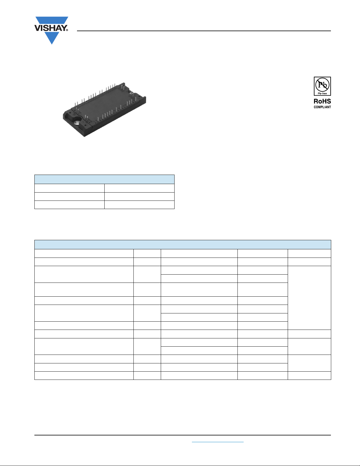
ECONO2 4PACK
PRODUCT SUMMARY
V
CES
at TC = 67 °C 75 A
I
C
V
(typical) 3.4 V
CE(on)
Vishay High Power Products
IGBT Fourpack Module, 75 A
FEATURES
• Square RBSOA
®
low Qrr, low switching energy
temperature coefficient
CE(on)
1200 V
•HEXFRED
•Positive V
• Copper baseplate
• Low stray inductance design
• Speed 8 kHz to 60 kHz
• Compliant to RoHS directive 2002/95/EC
BENEFITS
• Benchmark efficiency for SMPS appreciation in particular
HF welding
• Rugged transient performance
• Low EMI, requires less snubbing
• Direct mounting to heatsink space saving
• PCB solderable terminals
GB75YF120UT
• Low junction to case thermal resistance
ABSOLUTE MAXIMUM RATINGS
PARAMETER SYMBOL TEST CONDITIONS MAX. UNITS
Collector to emitter voltage V
Continuous collector current I
Pulsed collector current
See fig. C.T.5
Clamped inductive load current I
Diode continuous forward current I
Diode maximum forward current I
Gate to emitter voltage V
Maximum power dissipation (IGBT) P
Maximum operating junction temperature T
Storage temperature range T
Isolation voltage V
CES
I
CM
LM
FM
Stg
ISOL
C
F
GE
TC = 25 °C 100
= 80 °C 67
T
C
TC = 25 °C 60
= 80 °C 40
T
C
TC = 25 °C 480
D
T
= 80 °C 270
C
J
1200 V
200
200
150
± 20 V
150
- 40 to + 125
AC 2500 (MIN) V
A
W
°C
Document Number: 93172 For technical questions, contact: indmodules@vishay.com
Revision: 13-Jan-10 1
www.vishay.com
GB75YF120UT
Vishay High Power Products
IGBT Fourpack Module, 75 A
ELECTRICAL SPECIFICATIONS (TJ = 25 °C unless otherwise specified)
PARAMETER SYMBOL TEST CONDITIONS MIN. TYP. MAX. UNITS
Collector to emitter breakdown voltage V
Gate threshold voltage V
Threshold voltage temperature coefficient ΔV
GE(th)
Zero gate voltage collector current I
Diode forward voltage drop V
Gate to emitter leakage current I
BR(CES)
CE(ON)
GE(th)
CES
FM
GES
VGE = 0 V, IC = 500 μA 1200 - -
IC = 75 A, VGE = 15 V - 3.4 4.0
I
= 100 A, VGE = 15 V - 3.8 4.5
C
I
= 75 A, VGE = 15 V, TJ = 125 °C - 4.0 4.5
C
= 100 A, VGE = 15 V, TJ = 125 °C - 4.53 5.1
I
C
VCE = VGE, IC = 250 μA 4.0 5.0 6.0
/ΔTJVCE = VGE, IC = 1 mA (25 °C to 125 °C) - - 11 - mV/°C
VGE = 0 V, VCE = 1200 V - 7 250
V
= 0 V, VCE = 1200 V, TJ = 125 °C - 580 2000
GE
IF = 75 A - 3.7 4.9
= 100 A - 4.1 5.5
I
F
I
= 75 A, TJ = 125 °C - 3.7 5.1
F
I
= 100 A, TJ = 125 °C - 4.2 5.7
F
VGE = ± 20 V - - ± 200 nA
VCollector to emitter voltage V
μA
V
SWITCHING CHARACTERISTICS (T = 25 °C unless otherwise noted)
PARAMETER SYMBOL TEST CONDITIONS MIN. TYP. MAX. UNITS
Total gate charge (turn-on) Q
Gate to collector charge (turn-on) Q
Turn-on switching loss E
Turn-off switching loss E
Total switching loss E
Turn-on switching loss E
Turn-off switching loss E
Total switching loss E
Turn-on delay time t
Rise time t
Turn-off delay time t
Fall time t
Reverse bias safe operating area RBSOA
Short circuit safe operating area SCSOA
Diode peak reverse recovery current I
Diode reverse recovery time t
Total reverse recovery charge Q
Note
(1)
Energy losses include “tail” and diode reverse recovery
GE
GC
on
off
tot
on
off
tot
d(on)
d(off)
rr
rr
G
IC = 75 A
= 600 V
V
CC
= 15 V
V
GE
IC = 75 A, VCC = 600 V
= 15 V, Rg = 5 Ω, L = 500 μH
V
GE
T
= 25 °C
J
(1)
IC = 75 A, VCC = 600 V
= 15 V, Rg = 5 Ω, L = 500 μH
V
GE
T
= 125 °C
J
r
f
IC = 75 A, VCC = 600 V
V
= 15 V, Rg = 5 Ω, L = 500 μH
GE
= 125 °C
T
J
= 150 °C, IC = 200 A
T
J
R
= 10 Ω, VGE = 15 V to 0 V
g
= 150 °C
T
J
V
= 900 V, VP = 1200 V
CC
R
= 10 Ω, VGE = 15 V to 0 V
g
(1)
TJ = 25 °C
T
= 125 °C - 19 23
J
TJ = 25 °C - 132 189
T
= 125 °C - 200 270
J
= 200 V
V
CC
I
= 50 A
F
dI/dt = 10 A/μs
TJ = 25 °C - 858 1700
rr
T
= 125 °C - 1900 3105
J
- 630 -
-65-
- 250 -
-1.74-
-1.46-
-3.20-
-2.44-
-2.35-
-4.79-
- 268 -
-43-
- 308 -
- 127 -
Fullsquare
10 - - μs
-1318
nCGate to emitter charge (turn-on) Q
mJ
ns
A
ns
nC
www.vishay.com For technical questions, contact: indmodules@vishay.com Document Number: 93172
2 Revision: 13-Jan-10
GB75YF120UT
IGBT Fourpack Module, 75 A
Vishay High Power Products
THERMISTOR ELECTRICAL SPECIFICATIONS (T = 25 °C unless otherwise specified)
PARAMETER SYMBOL TEST CONDITIONS MIN. TYP. MAX. UNITS
Resistance R
25
B value B T
4538 5000 5495
T
= 100 °C 468.6 493.3 518
J
= 25 °C/50 °C 3307 3375 3443 °K
J
Ω
THERMAL AND MECHANICAL SPECIFICATIONS
PARAMETER SYMBOL MIN. TYP. MAX. UNITS
Junction to case IGBT R
Case to sink, flat, greased surface R
Mounting torque (M5) 2.7 - 3.3 Nm
Weight - 170 - g
160
140
120
100
(°C)
80
C
T
60
40
20
0
0 20406080100120
IC (A)
Fig. 1 - Maximum DC Collector Current vs.
Case Temperature
(IGBT) - - 0.26
thJC
(DIODE) - - 0.56
thJC
(MODULE) - 0.02 -
thCS
1000
100
10
IC (A)
1
0.1
0.01
1 10 100 1000 10000
Fig. 3 - Forward SOA
T
= 25 °C; TJ ≤ 150 °C
C
°C/WJunction to case DIODE R
VCE (V)
500
400
300
(W)
D
P
200
100
0
0 20406080100120140160
TC (°C)
Fig. 2 - Power Dissipation vs. Case Temperature
1000
100
(A)
C
I
10
1
10 100 1000 10000
VCE (V)
Fig. 4 - Reverse Bias SOA
= 150 °C; VGE = 15 V
T
J
Document Number: 93172 For technical questions, contact: indmodules@vishay.com
www.vishay.com
Revision: 13-Jan-10 3
GB75YF120UT
Vishay High Power Products
160
VGE = 18V
VGE = 15V
140
VGE = 12V
VGE = 9V
120
100
(A)
80
CE
I
60
40
20
0
0123456
VCE (V)
Fig. 5 - Typical IGBT Output Characteristics
160
140
120
100
(A)
80
CE
I
60
40
20
0
012345678
Fig. 6 - Typical IGBT Output Characteristics
T
VGE = 18V
VGE = 15V
VGE = 12V
VGE = 9V
T
= 25 °C; tp = 500 μs
J
VCE (V)
= 125 °C; tp = 500 μs
J
IGBT Fourpack Module, 75 A
20
18
16
14
12
(V)
10
CE
V
8
6
4
2
0
7 9 11 13 15 17 19
Fig. 8 - Typical V
20
18
16
14
12
(V)
10
CE
V
8
6
4
2
0
7 9 11 13 15 17 19
Fig. 9 - Typical V
VGE (V)
TJ = 25 °C
VGE (V)
TJ = 125 °C
CE
CE
vs. V
vs. V
ICE = 75A
ICE= 50A
ICE= 25A
GE
ICE = 75A
ICE= 50A
ICE= 25A
GE
150
140
130
120
110
100
90
80
(A)
F
I
70
60
50
Tj = 25°C
40
Tj = 125°C
30
20
10
0
0.0 1.0 2.0 3.0 4.0 5.0
VF (V)
Fig. 7 - Typical Diode Forward Characteristics
= 500 μs
t
p
300
TJ = 25°C
250
200
(A)
150
CE
I
100
50
0
56789101112
TJ= 125°C
VGE (V)
Fig. 10 - Typical Transfer Characteristics
= 20 V; tp = 500 μs
V
CE
www.vishay.com For technical questions, contact: indmodules@vishay.com Document Number: 93172
4 Revision: 13-Jan-10

0
GB75YF120UT
IGBT Fourpack Module, 75 A
1
TJ= 125°C
0.1
(mA)
CES
I
0.01
TJ = 25°C
0.001
400 600 800 1000 1200
V
(V)
CES
Fig. 11 - Typical Zero Gate Voltage Collector Current
5.5
5
TJ = 25°C
TJ= 125°C
(V)
geth
V
4.5
4
3.5
3
Vishay High Power Products
1000
100
t
Switching Time (ns)
10
20 30 40 50 60 70 80
Fig. 14 - Typical Switching Time vs. I
TJ = 125 °C; L = 500 μH; V
14000
12000
10000
J)
8000
6000
Energy (μ
4000
R
E
td
OFF
td
ON
t
F
IC (A)
= 600 V, Rg = 5 Ω; VGE = 15 V
CC
ON
E
OFF
C
2.5
2
0 0.2 0.4 0.6 0.8 1
IC (mA)
Fig. 12 - Typical Threshold Voltage
2500
2000
E
ON
E
Energy (μJ)
1500
1000
30 40 50 60 70 80
Fig. 13 - Typical Energy Loss vs. I
TJ = 125 °C; L = 500 μH; VCC = 600 V, Rg = 5 Ω; V
OFF
IC (A)
C
GE
= 15 V
2000
0
0 1020304050
RG ( Ω)
TJ = 125 °C; L = 500 μH; VCC = 600 V, IC = 75 A; V
Fig. 15 - Typical Energy Loss vs. R
10000
1000
td
OFF
100
Switching Time (ns)
10
0 10 20 30 40 5
td
ON
t
F
t
R
g
RG ( Ω)
Fig. 16 - Typical Switching Time vs. R
TJ = 125 °C; L = 500 μH; V
= 600 V, IC = 75 A; VGE = 15 V
CC
= 15 V
GE
g
Document Number: 93172 For technical questions, contact: indmodules@vishay.com www.vishay.com
Revision: 13-Jan-10 5

GB75YF120UT
0
Vishay High Power Products
120
100
80
(A)
60
RR
I
40
20
0
10 15 20 25 30 35 40 45 50 55 60 65 70 75 80
Fig. 17 - Typical Diode IRR vs. I
100
80
60
(A)
RR
I
40
20
0
400 800 1200 1600 2000
Fig. 18 - Typical Diode I
V
5 ohm
IF(A)
TJ = 125 °C
/ dt (A/ μs)
dI
F
= 600 V; IF = 75 A
CC
27 ohm
47 ohm
vs. dIF/dt
RR
IGBT Fourpack Module, 75 A
100
80
60
(A)
RR
I
40
20
F
16
14
12
10
(V)
GE
V
0
0 10 20 30 40 5
RG ( Ω)
Fig. 19 - Typical Diode I
TJ = 125 °C; IF = 75 A
8
6
4
2
0
0 100 200 300 400 500 600 700
, Total Gate Charge (nC)
Q
G
vs. R
RR
typical value
Fig. 20 - Typical Gate Charge vs. V
I
= 5.0 A; L = 600 μH
CE
g
GE
1
D = 0.50
0.1
)
thJC
0.01
0.001
0.0001
Thermal Response (Z
1E-005
1E-006 1E-005 0.0001 0.001 0.01 0.1 1 10
0.20
0.10
0.05
0.02
0.01
SINGLE PULSE
( THERMAL RESPONSE )
t1, Rectangular Pulse Duration (sec)
Fig. 21 - Maximum Transient Thermal Impedance, Junction to Case (IGBT)
www.vishay.com For technical questions, contact: indmodules@vishay.com Document Number: 93172
6 Revision: 13-Jan-10

GB75YF120UT
0
1K
D.U.T.
Fig. C.T.1 - Gate Charge Circuit (Turn-Off)
L
80 V
+
-
R
g
D.U.T.
IGBT Fourpack Module, 75 A
L
1000 V
V
CC
+
-
Vishay High Power Products
Driver
D
+
900 V
-
+
-
V
CC
Fig. C.T.3 - S.C. SOA Circuit
Diode clamp/
D.U.T.
+
-
- 5 V
R
g
C
D.U.T.
L
D.U.T./
Driver
Fig. C.T.2 - RBSOA Circuit
V
CC
R =
I
CM
D.U.T.
R
g
Fig. C.T.4 - Switching Loss Circuit
+
-
V
CC
Fig. C.T.5 - Resistive Load Circuit
Document Number: 93172 For technical questions, contact: indmodules@vishay.com www.vishay.com
Revision: 13-Jan-10 7

GB75YF120UT
Vishay High Power Products
ORDERING INFORMATION TABLE
Device code
CIRCUIT CONFIGURATION
G B 75 Y F 120 U T
1 - Insulated gate bipolar transistor (IGBT)
2 - B = IGBT Generation 5
3 - Current rating (75 = 75 A)
4 - Circuit configuration (Y = Fourpack)
5 - Package indicator (F = ECONO2)
6 - Voltage rating (120 = 1200 V)
7 - Speed/type (U = Ultrafast IGBT)
8 - T = Thermistor
C1
48 49
IGBT Fourpack Module, 75 A
51324
678
21 22
C2
QB1
41
G1
Aux1
43
QB2
G2
37
Aux2
38
46 47
E1
Dimensions www.vishay.com/doc?95252
5
C/E1
6
7
10 12
RT1
LINKS TO RELATED DOCUMENTS
G3
Aux3
G4
Aux4
28
29
32
33
QB3
QB4
23 24
E2
15
C/E2
16
17
www.vishay.com For technical questions, contact: indmodules@vishay.com Document Number: 93172
8 Revision: 13-Jan-10

DIMENSIONS in millimeters (inches)
Z
Y
20.5
+ 1.0
- 0.5
105 ± 0.1
13.2 ± 0.15
0.8
1.25
- 0.02
- 0.06
0.8 ± 0.03
X 2:1
34.29
30.48
22.86
19.05
30.48
22.86
19.05
34.29
30.48
22.86
19.05
26.67
39.49
93 ± 0.15
107.8 ± 0.2
22.86
19.05
26.67
34.29
39.49
15.24
21 ± 0.03
21 ± 0.03
5.5 ± 0.05
10.5
45.4 ± 0.2
42 ± 0.15
7.5
0
- 0 3
11.43
Detail
R 3
10.5
83
0
- 0.2
Z 2:1
0.6
0.5
0.8 ± 0.03
Y 2:1
0.85
1
1.25
- 0.02
- 0.06
2
49
4
5
6
7
810
12
15
16
17
19
48
47
46
44
43
41
40
38
37
36
35
33
32
30
2928
27
26
24
23
22
21
11.43
7.62
7.62
11.43
11.43
7.62
7.62
3.81
7.62
7.62
11.43
ECONO2 4PAK
Outline Dimensions
Vishay Semiconductors
Document Number: 95252 For technical questions, contact: indmodules@vishay.com
www.vishay.com
Revision: 29-Nov-07 1

Legal Disclaimer Notice
Vishay
Disclaimer
ALL PRODUCT, PRODUCT SPECIFICATIONS AND DATA ARE SUBJECT TO CHANGE WITHOUT NOTICE TO IMPROVE
RELIABILITY, FUNCTION OR DESIGN OR OTHERWISE.
Vishay Intertechnology, Inc., its affiliates, agents, and employees, and all persons acting on its or their behalf (collectively,
“Vishay”), disclaim any and all liability for any errors, inaccuracies or incompleteness contained in any datasheet or in any other
disclosure relating to any product.
Vishay makes no warranty, representation or guarantee regarding the suitability of the products for any particular purpose or
the continuing production of any product. To the maximum extent permitted by applicable law, Vishay disclaims (i) any and all
liability arising out of the application or use of any product, (ii) any and all liability, including without limitation special,
consequential or incidental damages, and (iii) any and all implied warranties, including warranties of fitness for particular
purpose, non-infringement and merchantability.
Statements regarding the suitability of products for certain types of applications are based on Vishay’s knowledge of typical
requirements that are often placed on Vishay products in generic applications. Such statements are not binding statements
about the suitability of products for a particular application. It is the customer’s responsibility to validate that a particular
product with the properties described in the product specification is suitable for use in a particular application. Parameters
provided in datasheets and/or specifications may vary in different applications and performance may vary over time. All
operating parameters, including typical parameters, must be validated for each customer application by the customer’s
technical experts. Product specifications do not expand or otherwise modify Vishay’s terms and conditions of purchase,
including but not limited to the warranty expressed therein.
Except as expressly indicated in writing, Vishay products are not designed for use in medical, life-saving, or life-sustaining
applications or for any other application in which the failure of the Vishay product could result in personal injury or death.
Customers using or selling Vishay products not expressly indicated for use in such applications do so at their own risk and agree
to fully indemnify and hold Vishay and its distributors harmless from and against any and all claims, liabilities, expenses and
damages arising or resulting in connection with such use or sale, including attorneys fees, even if such claim alleges that Vishay
or its distributor was negligent regarding the design or manufacture of the part. Please contact authorized Vishay personnel to
obtain written terms and conditions regarding products designed for such applications.
No license, express or implied, by estoppel or otherwise, to any intellectual property rights is granted by this document or by
any conduct of Vishay. Product names and markings noted herein may be trademarks of their respective owners.
Document Number: 91000 www.vishay.com
Revision: 11-Mar-11 1
 Loading...