

ECONO2 4PACK
PRODUCT SUMMARY
V
CES
at TC = 67 °C 75 A
I
C
V
(typical) 3.4 V
CE(on)
Vishay High Power Products
IGBT Fourpack Module, 75 A
FEATURES
• Square RBSOA
®
low Qrr, low switching energy
temperature coefficient
CE(on)
1200 V
• HEXFRED
•Positive V
• Copper baseplate
• Low stray inductance design
• Speed 8 to 60 kHz
• Designed and qualified for industrial market
BENEFITS
• Benchmark efficiency for SMPS appreciation in particular
HF welding
• Rugged transient performance
• Low EMI, requires less snubbing
• Direct mounting to heatsink space saving
• PCB solderable terminals
• Low junction to case thermal resistance
GB75YF120N
RoHS
COMPLIANT
ABSOLUTE MAXIMUM RATINGS
PARAMETER SYMBOL TEST CONDITIONS MAX. UNITS
Collector to emitter voltage V
Continuous collector current I
Pulsed collector current
See fig. C.T.5
Clamped inductive load current I
Diode continuous forward current I
Diode maximum forward current I
Gate to emitter voltage V
Maximum power dissipation (IGBT) P
Maximum operating junction temperature T
Storage temperature range T
Isolation voltage V
CES
I
CM
LM
FM
ISOL
Stg
C
F
GE
TC = 25 °C 100
= 80 °C 67
T
C
TC = 25 °C 40
T
= 80 °C 25
C
TC = 25 °C 480
D
T
= 80 °C 270
C
J
1200 V
200
200
150
± 20 V
150
- 40 to + 125
AC 2500 (MIN) V
A
W
°C
Document Number: 93654 For technical questions, contact: ind-modules@vishay.com
Revision: 01-Sep-08 1
www.vishay.com
GB75YF120N
Vishay High Power Products
IGBT Fourpack Module, 75 A
ELECTRICAL SPECIFICATIONS (TJ = 25 °C unless otherwise specified)
PARAMETER SYMBOL TEST CONDITIONS MIN. TYP. MAX. UNITS
Collector to emitter breakdown voltage V
Gate threshold voltage V
Threshold voltage temperature coefficient ΔV
GE(th)
Zero gate voltage collector current I
Diode forward voltage drop V
Gate to emitter leakage current I
BR(CES)
CE(ON)
GE(th)
CES
FM
GES
VGE = 0 V, IC = 500 µA 1200 - -
IC = 75 A, VGE = 15 V - 3.4 4.0
I
= 100 A, VGE = 15 V - 3.8 4.5
C
I
= 75 A, VGE = 15 V, TJ = 125 °C - 4.0 4.5
C
= 100 A, VGE = 15 V, TJ = 125 °C - 4.53 5.1
I
C
VCE = VGE, IC = 250 µA 4.0 5.0 6.0
/ΔTJVCE = VGE, IC = 1 mA (25 °C to 125 °C) - - 11 - mV/°C
VGE = 0 V, VCE = 1200 V - 7 250
V
= 0 V, VCE = 1200 V, TJ = 125 °C - 580 2000
GE
IF = 75 A - 3.9 5.0
= 100 A - 4.43 5.8
I
F
I
= 75 A, TJ = 125 °C - 4.37 5.4
F
I
= 100 A, TJ = 125 °C - 5.02 6.4
F
VGE = ± 20 V - - ± 200 nA
VCollector to emitter voltage V
µA
V
SWITCHING CHARACTERISTICS (TJ = 25 °C unless otherwise noted)
PARAMETER SYMBOL TEST CONDITIONS MIN. TYP. MAX. UNITS
Total gate charge (turn-on) Q
Gate to collector charge (turn-on) Q
Turn-on switching loss E
Turn-off switching loss E
Total switching loss E
Turn-on switching loss E
Turn-off switching loss E
Total switching loss E
Turn-on delay time t
Rise time t
Turn-off delay time t
Fall time t
Reverse bias safe operating area RBSOA
Short circuit safe operating area SCSOA
Diode peak reverse recovery current I
Diode reverse recovery time t
Total reverse recovery charge Q
GE
GC
on
off
tot
on
off
tot
d(on)
d(off)
rr
rr
G
IC = 500 A
= 600 V
V
CC
= 15 V
V
GE
IC = 50 A, VCC = 600 V
= 15 V, RG = 4.7 Ω, L = 500 µH
V
GE
T
= 25 °C
J
(1)
IC = 50 A, VCC = 600 V
= 15 V, RG = 4.7 Ω, L = 500 µH
V
GE
T
= 125 °C
J
r
f
IC = 50 A, VCC = 600 V
V
GE
= 125 °C
T
J
= 150 °C, IC = 150 A
T
J
R
= 10 Ω, VGE = 15 V to 0 V
G
= 150 °C
T
J
V
CC
R
= 10 Ω, VGE = 15 V to 0 V
G
(1)
= 15 V, RG = 4.7 Ω, L = 500 µH
= 900 V, VP = 1200 V
TJ = 25 °C
T
= 125 °C - 2.35 4.0
J
TJ = 25 °C - 0.401 0.5
T
= 125 °C - 0.655 0.8
J
= 600 V
V
CC
I
= 75 A
F
dI/dt = 10 A/µs
TJ = 25 °C - 0.181 0.4
rr
T
= 125 °C - 0.54 1.5
J
Note
(1)
Energy losses include “tail” and diode reverse recovery
www.vishay.com For technical questions, contact: ind-modules@vishay.com
2 Revision: 01-Sep-08
- 630 -
-65-
nCGate to emitter charge (turn-on) Q
- 250 -
-1.51-
-2.41-
-3.92-
-2.25-
mJ
-3.35-
-7.60-
- 169 -
-71-
- 393 -
ns
- 136 -
Fullsquare
10 - - µs
- 1.45 2.5
µs
µC
Document Number: 93654
A
GB75YF120N
IGBT Fourpack Module, 75 A
Vishay High Power Products
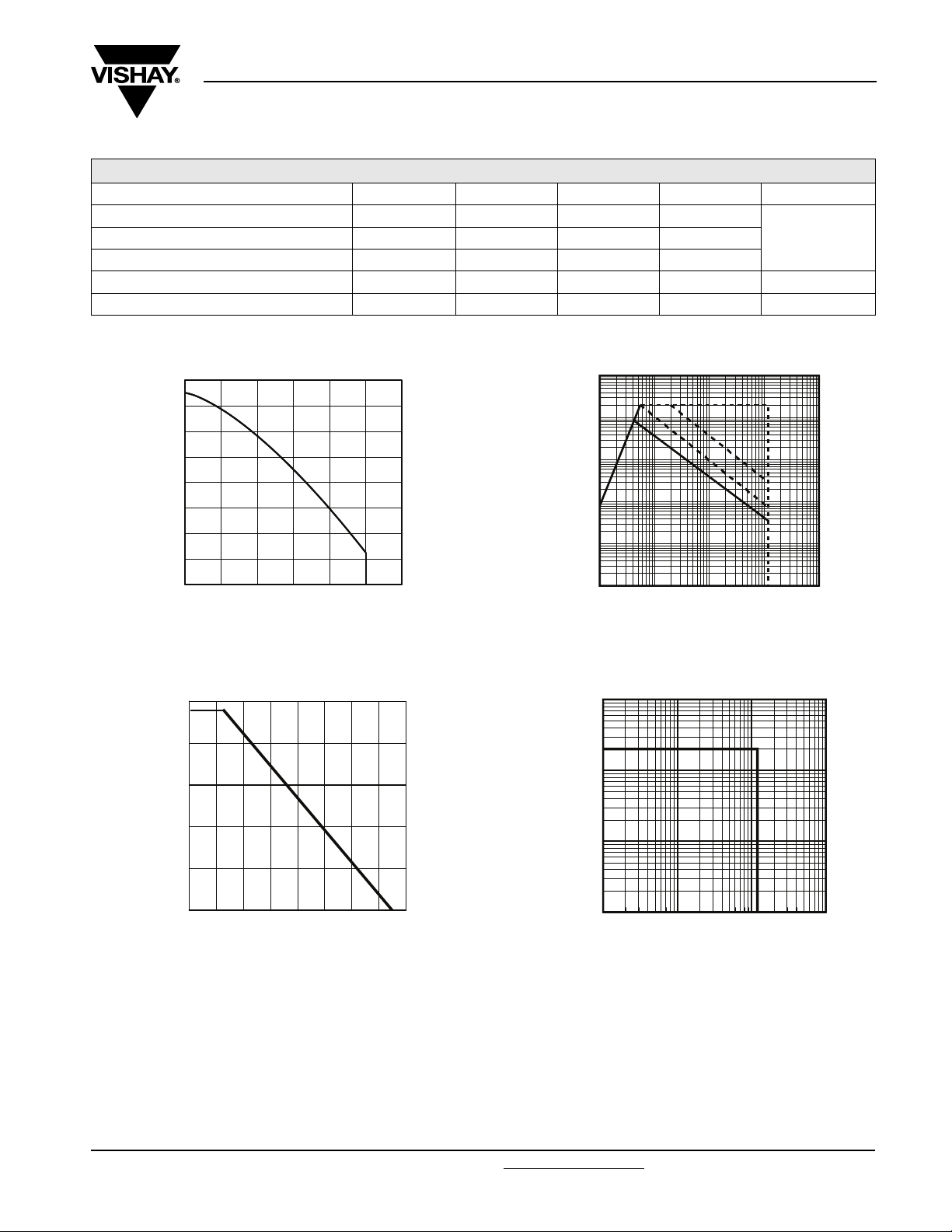
THERMAL AND MECHANICAL SPECIFICATIONS
PARAMETER SYMBOL MIN. TYP. MAX. UNITS
Junction to case IGBT R
Case to sink, flat, greased surface R
Mounting torque (M5) 2.7 - 3.3 Nm
Weight - 170 - g
160
140
120
100
(A)
80
C
I
60
40
20
0
0 20406080100120
TC (°C)
Fig. 1 - Maximum DC Collector Current vs.
Case Temperature
(IGBT) - - 0.26
thJC
(DIODE) - - 1.00
thJC
(MODULE) - 0.05 -
thCS
1000
100
10
IC (A)
1
0.1
0.01
1 10 100 1000 10000
Fig. 3 - Forward SOA
T
= 25 °C; TJ ≤ 150 °C
C
°C/WJunction to case DIODE R
VCE (V)
500
400
300
(W)
D
P
200
100
0
0 20 40 60 80 100 120 140 160
TC (°C)
Fig. 2 - Power Dissipation vs. Case Temperature
1000
100
(W)
D
P
10
1
10 100 1000 10000
TC (°C)
Fig. 4 - Reverse Bias SOA
= 150 °C; VGE = 15 V
T
J
Document Number: 93654 For technical questions, contact: ind-modules@vishay.com
www.vishay.com
Revision: 01-Sep-08 3
 Loading...