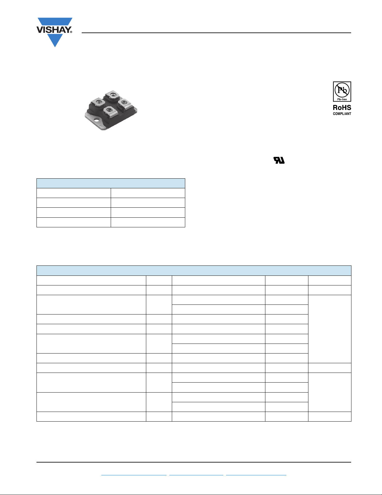
"High Side Chopper" IGBT SOT-227
(Warp 2 Speed IGBT), 70 A
FEATURES
• NPT warp 2 speed IGBT technology with
positive temperature coefficient
• Square RBSOA
SOT-227
•Low V
•FRED Pt® hyperfast rectifier
• Fully isolated package
• Very low internal inductance ( 5 nH typical)
• Industry standard outline
• UL approved file E78996
• Compliant to RoHS directive 2002/95/EC
CE(on)
GB70NA60UF
Vishay Semiconductors
PRODUCT SUMMARY
V
CES
DC 70 A at 88 °C
I
C
typical at 70 A, 25 °C 2.4 V
V
CE(on)
DC 70 A at 86 °C
I
F
600 V
BENEFITS
• Designed for increased operating efficiency in power
conversion: UPS, SMPS, welding, induction heating
• Easy to assemble and parallel
• Direct mounting to heatsink
• Plug-in compatible with other SOT-227 packages
• Higher switching frequency up to 150 kHz
• Lower conduction losses and switching losses
• Low EMI, requires less snubbing
ABSOLUTE MAXIMUM RATINGS
PARAMETER SYMBOL TEST CONDITIONS MAX. UNITS
Collector to emitter voltage V
Continuous collector current I
Pulsed collector current I
Clamped inductive load current I
Diode continuous forward current I
Peak diode forward current I
Gate to emitter voltage V
Power dissipation, IGBT P
Power dissipation, diode P
RMS isolation voltage V
CES
C
CM
LM
F
FM
GE
D
D
ISOL
TC = 25 °C 111
= 80 °C 76
T
C
TC = 25 °C 113
= 80 °C 75
T
C
TC = 25 °C 447
= 80 °C 250
T
C
TC = 25 °C 236
= 80 °C 132
T
C
Any terminal to case, t = 1 min 2500 V
600 V
120
120
200
± 20 V
A
W
Document Number: 93103 For technical questions within your region, please contact one of the following: www.vishay.com
Revision: 22-Jul-10 DiodesAmericas@vishay.com
, DiodesAsia@vishay.com, DiodesEurope@vishay.com 1

GB70NA60UF
Vishay Semiconductors
"High Side Chopper" IGBT SOT-227
(Warp 2 Speed IGBT), 70 A
ELECTRICAL SPECIFICATIONS (TJ = 25 °C unless otherwise specified)
PARAMETER SYMBOL TEST CONDITIONS MIN. TYP. MAX. UNITS
Collector to emitter breakdown
voltage
V
Collector to emitter voltage V
Gate threshold voltage V
Temperature coefficient of
threshold voltage
V
GE(th)
Collector to emitter leakage current I
Diode reverse breakdown voltage V
Diode forward voltage drop V
Diode reverse leakage current I
Gate to emitter leakage current I
BR(CES)
CE(on)
GE(th)
CES
BR
FM
RM
GES
VGE = 0 V, IC = 1 mA 600 - -
VGE = 15 V, IC = 35 A - 1.69 1.88
= 15 V, IC = 70 A - 2.23 2.44
V
GE
= 15 V, IC = 35 A, TJ = 125 °C - 2.07 2.31
V
GE
V
= 15 V, IC = 70 A, TJ = 125 °C - 2.89 3.21
GE
VCE = VGE, IC = 500 μA 3 3.9 5
/TJVCE = VGE, IC = 1 mA (25 °C to 125 °C) - - 9 - mV/°C
VGE = 0 V, VCE = 600 V - 1 100 μA
V
= 0 V, VCE = 600 V, TJ = 125 °C - 0.07 2.0 mA
GE
IR = 1 mA 600 - - V
IC = 35 A, VGE = 0 V - 1.80 2.33
= 70 A, VGE = 0 V - 2.13 2.71
I
C
= 35 A, VGE = 0 V, TJ = 125 °C - 1.35 1.81
I
C
I
= 70 A, VGE = 0 V, TJ = 125 °C - 1.70 2.32
C
VR = VR rated - 0.1 50 μA
= 125 °C, VR = VR rated - 0.02 3 mA
T
J
VGE = ± 20 V - - ± 200 nA
V
V
SWITCHING CHARACTERISTICS (TJ = 25 °C unless otherwise specified)
PARAMETER SYMBOL TEST CONDITIONS MIN. TYP. MAX. UNITS
Total gate charge (turn-on) Q
Gate to collector charge (turn-on) Q
Turn-on switching loss E
Turn-off switching loss E
Total switching loss E
Turn-on switching loss E
Turn-off switching loss E
Total switching loss E
Turn-on delay time t
Rise time t
Turn-off delay time t
Fall time t
Reverse bias safe operating area RBSOA
Diode reverse recovery time t
Diode peak reverse current I
Diode recovery charge Q
Diode reverse recovery time t
Diode peak reverse current I
Diode recovery charge Q
on
off
tot
on
off
tot
d(on)
d(off)
rr
rr
rr
rr
g
IC = 50 A, VCC = 400 V, VGE = 15 V
ge
gc
IC = 70 A, VCC = 360 V,
V
= 15 V, Rg = 5
GE
L = 500 μH, T
= 25 °C
J
IC = 70 A, VCC = 360 V,
= 15 V, Rg = 5
V
GE
r
f
L = 500 μH, T
= 150 °C, IC = 120 A, Rg = 22
T
J
= 15 V to 0 V, VCC = 400 V,
V
GE
= 600 V
V
P
= 125 °C
J
IF = 50 A, dIF/dt = 200 A/μs, VR = 200 V
rr
IF = 50 A, dIF/dt = 200 A/μs,
V
= 200 V, TJ = 125 °C
rr
R
Energy losses
include tail and
diode recovery
(see fig. 18)
www.vishay.com For technical questions within your region, please contact one of the following: Document Number: 93103
2 DiodesAmericas@vishay.com
, DiodesAsia@vishay.com, DiodesEurope@vishay.com Revision: 22-Jul-10
- 320 -
-42-
nCGate to emitter charge (turn-on) Q
- 110 -
-1.15-
-1.16-
-2.31-
-1.27-
mJ
-1.28-
-2.55-
- 208 -
-69-
- 208 -
ns
- 100 -
Fullsquare
-5993ns
-46A
- 118 279 nC
- 130 159 ns
-1113A
- 715 995 nC

Allowable Case Temperature (°C)
IC - Continuous Collector Current (A)
0 20406080 120100
0
160
100
120
140
20
40
60
80
I
C
(A)
VCE (V)
1 10 100 1000
0.01
0.1
1
1000
10
100
I
CES
(mA)
V
CES
(V)
100 200 300 400 500 600
0.0001
1
0.01
0.1
0.001
TJ = 125 °C
TJ = 25 °C
GB70NA60UF
"High Side Chopper" IGBT SOT-227
Vishay Semiconductors
(Warp 2 Speed IGBT), 70 A
THERMAL AND MECHANICAL SPECIFICATIONS
PARAMETER SYMBOL MIN. TYP. MAX. UNITS
Maximum junction and
storage temperature range
Thermal resistance, junction to case
IGBT
Thermal resistance, case to sink per module R
Mounting torque, 6-32 or M3 screw - - 1.3 Nm
Weight -30-g
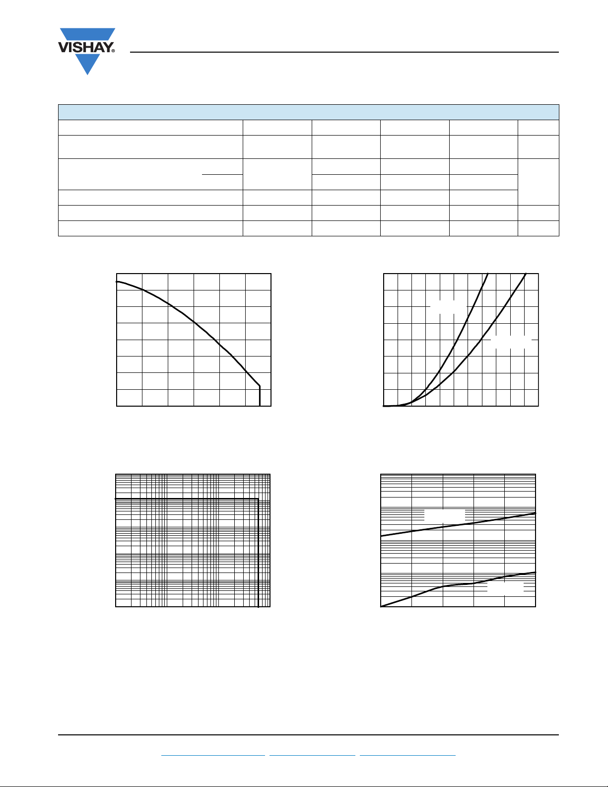
Fig. 1 - Maximum DC IGBT Collector Current vs.
Case Temperature
, T
T
J
Stg
R
thJC
thCS
- 40 - 150 °C
- - 0.28
°C/WDiode - - 0.53
-0.05-
200
175
TJ = 25 °C
TJ = 125 °C
(A)
C
I
150
125
100
75
50
25
0
024135
VCE (V)
Fig. 3 - Typical IGBT Collector Current Characteristics
Document Number: 93103 For technical questions within your region, please contact one of the following: www.vishay.com
Revision: 22-Jul-10 DiodesAmericas@vishay.com
Fig. 2 - IGBT Reverse Bias SOA
T
= 150 °C, VGE = 15 V
J
Fig. 4 - Typical IGBT Zero Gate Voltage Collector Current
, DiodesAsia@vishay.com, DiodesEurope@vishay.com 3
 Loading...