INT-A-PAK
PRODUCT SUMMARY
V
CES
DC 220 A
I
C
at 100 A, 25 °C 1.11 V
V
CE(on)
Vishay High Power Products
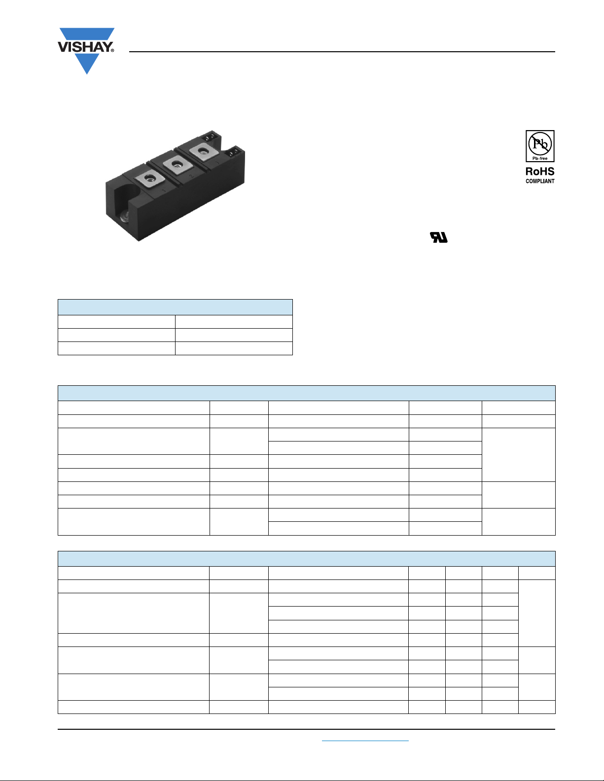
"Half-Bridge" IGBT INT-A-PAK
(Standard Speed IGBT), 100 A
FEATURES
• Standard speed PT IGBT technology
• Standard speed: DC to 1 kHz, optimized for
hard switching speed
2O3
®
antiparallel diodes with fast recovery
DBC
600 V
•FRED Pt
• Very low conduction losses
•Al
• UL approved file E78996
• Compliant to RoHS directive 2002/95/EC
• Designed for industrial level
BENEFITS
• Optimized for high current inverter stages (AC TIG welding
machines)
• Direct mounting to heatsink
• Very low junction to case thermal resistance
•Low EMI
GA100TS60SFPbF
ABSOLUTE MAXIMUM RATINGS
PARAMETER SYMBOL TEST CONDITIONS MAX. UNITS
Collector to emitter voltage V
Continuous collector current I
Pulsed collector current I
Peak switching current I
Gate to emitter voltage V
RMS isolation voltage V
Maximum power dissipation P
CES
C
CM
LM
GE
ISOL
D
TC = 25 °C 220
= 130 °C 100
T
C
Any terminal to case, t = 1 min 2500
TC = 25 °C 780
T
= 100 °C 312
C
600 V
440
440
± 20
A
V
W
ELECTRICAL SPECIFICATIONS (TJ = 25 °C unless otherwise specified)
PARAMETER SYMBOL TEST CONDITIONS MIN. TYP. MAX. UNITS
Collector to emitter breakdown voltage V
Gate threshold voltage V
Collector to emitter leakage current I
Diode forward voltage drop V
Gate to emitter leakage current I
Document Number: 94544 For technical questions, contact: indmodules@vishay.com
Revision: 04-May-10 1
BR(CES)
CE(on)
GE(th)
CES
FM
GES
VGE = 0 V, IC = 1 mA 600 - -
VGE = 15 V, IC = 100 A - 1.11 1.28
= 200 A - 1.39 -
I
C
= 15 V, IC = 100 A, TJ = 125 °C - 1.08 1.22
V
GE
IC = 0.25 mA 3 - 6
VGE = 0 V, VCE = 600 V - - 1
V
= 0 V, VCE = 600 V, TJ = 125 °C - - 10
GE
IC = 100 A, VGE = 0 V - 1.44 1.96
I
= 100 A, VGE = 0 V, TJ = 125 °C - 1.25 1.54
C
VGE = ± 20 V - - ± 250 nA
www.vishay.com
mA
VCollector to emitter voltage V
V

GA100TS60SFPbF
Vishay High Power Products
"Half-Bridge" IGBT INT-A-PAK
(Standard Speed IGBT), 100 A
SWITCHING CHARACTERISTICS (TJ = 25 °C unless otherwise specified)
PARAMETER SYMBOL TEST CONDITIONS MIN. TYP. MAX. UNITS
Total gate charge Q
Gate to collector charge Q
Rise time t
Fall time t
Turn-on switching energy E
Turn-off switching energy E
Total switching energy E
Turn-on switching energy E
Turn-off switching energy E
Total switching energy E
Input capacitance C
Reverse transfer capacitance C
Diode reverse recovery time t
Diode peak reverse current I
Diode recovery charge Q
Diode reverse recovery time t
Diode peak reverse current I
Diode recovery charge Q
ge
gc
on
off
on
off
ies
oes
res
rr
rr
rr
rr
g
r
f
ts
IC = 100 A
= 400 V
V
CC
= 15 V
V
GE
IC = 100 A
V
= 480 V
CC
= 15 V
V
GE
= 15 Ω
R
g
T
= 25 °C
J
IC = 100 A, VCC = 480 V
= 15 V, Rg = 15 Ω
V
GE
= 125 °C
T
ts
J
VGE = 0 V
= 30 V
V
CC
f = 1.0 MHz
IF = 50 A
dI
/dt = 200 A/μs
F
= 200 V
V
rr
RR
IF = 50 A
dI
/dt = 200 A/μs
F
V
= 200 V, TJ = 125 °C
rr
RR
- 640 700
- 108 120
- 230 300
-0.45-
-1.0-
-46
-2329
-2735
-612
-3540
-4152
- 16 250 -
- 1040 -
- 190 -
- 91 155 ns
-10.615 A
- 500 900 nC
- 180 344 ns
- 17 20.5 A
- 1633 2315 nC
nCGate to emitter charge Q
μs
mJ
pFOutput capacitance C
THERMAL AND MECHANICAL SPECIFICATIONS
PARAMETER SYMBOL MIN. TYP. MAX. UNITS
Operating junction temperature range T
Storage temperature range T
Junction to case
per switch
Case to sink per module R
Mounting torque
case to heatsink - - 4
case to terminal 1, 2, 3 - - 3
J
Stg
R
thJC
thCS
Weight - 185 - g
www.vishay.com For technical questions, contact: indmodules@vishay.com
2 Revision: 04-May-10
- 40 - 150
- 40 - 125
--0.16
-0.1 -
Document Number: 94544
°C
°C/Wper diode - - 0.48
Nm

GA100TS60SFPbF
"Half-Bridge" IGBT INT-A-PAK
(Standard Speed IGBT), 100 A
1000
Vge = 15V
100
Tj = 25˚C
, Collector-to-Emitter Current (A)
C
I
10
0.6 0.8 1 1.2 1.4 1.6 1.8
VCE, Collector-to-Emitter Voltage (V)
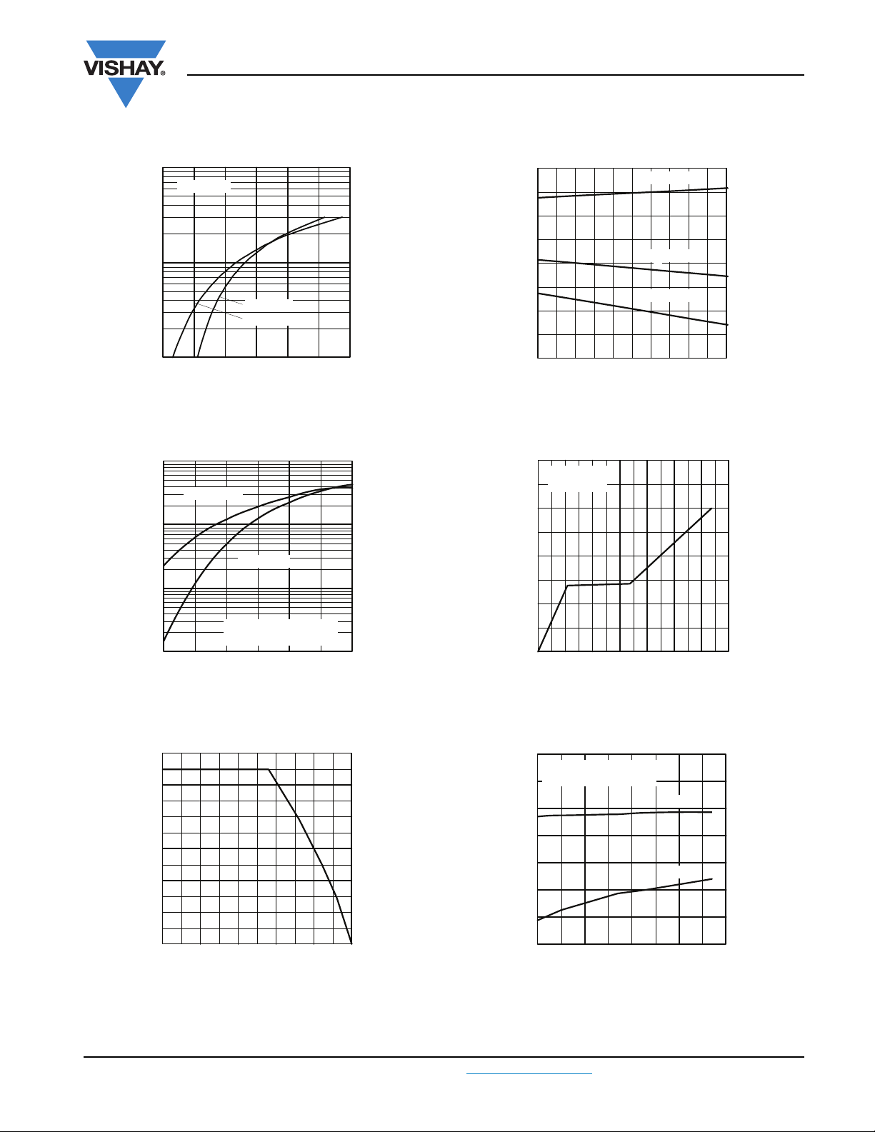
Fig. 1 - Typical Output Characteristics
1000
T = 125˚C
J
100
Tj = 125˚C
Vishay High Power Products
1.5
1.3
1.1
0.9
, Collector-to-Emitter Voltage (V)
CE
V
0.7
25 50 75 100 125 150
TJ, Junction Temperature (°C)
Fig. 4 - Typical Collector to Emitter Voltage vs.
Junction Temperature
20
Vcc = 400V
Ic = 100A
15
I = 200A
C
I = 100A
C
I = 50A
T = 25˚C
J
10
, Collector-to-Emitter Current (A)
C
I
Vce = 10V
380μs PULSE WIDTH
1
5.5 6.5 7.5 8.5
VGE, Gate-to-Emitter Voltage (V)
Fig. 2 - Typical Transfer Characteristics
240
200
160
120
80
40
Maximum DC Collector Current (A)
0
25 50 75 100 125 150
TC, Case Temperature (°C)
10
, Gate-to-Emitter Voltage (V)
5
GE
V
0
0 100 200 300 400 500 600 700
QG, Total Gate Charge (nC)
Fig. 5 - Typical Gate Charge vs.
Gate to Emitter Voltage
35
Tj = 25˚C, Vce = 480V
Vge = 15V, Ic = 100A
30
25
Eoff
20
15
10
Switching Losses (mJ)
Eon
5
0
10 20 30 40 50
RG, Gate Reistance (Ω)
Fig. 3 - Maximum Collector Current vs.
Case Temperature
Fig. 6 - Typical Switching Losses vs.
Gate Resistance
Document Number: 94544 For technical questions, contact: indmodules@vishay.com
www.vishay.com
Revision: 04-May-10 3
 Loading...