

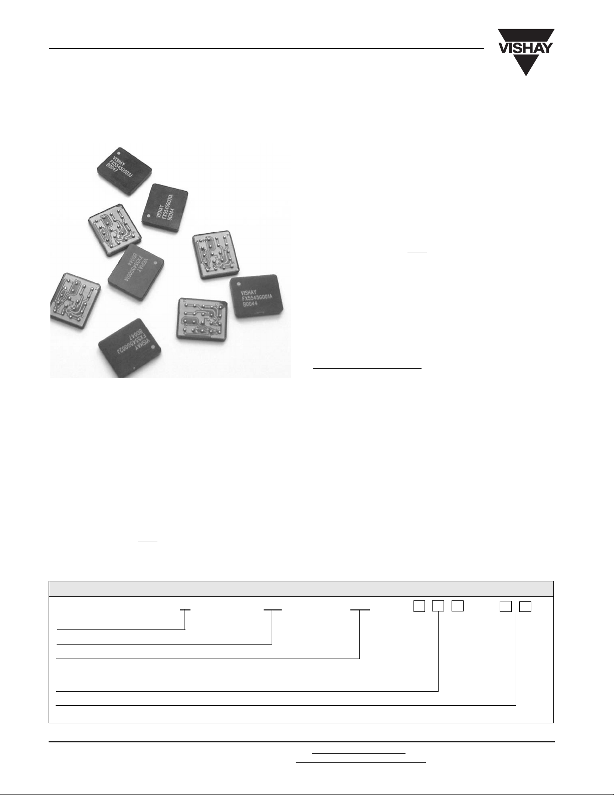
FX5545G008
Vishay
0.8V to 4.5V*, 3A with 380W/in
Low Profile 3mm DC/DC Buck Converter
3
Power Density
Efficiency up to 95%
FEATURES
• Fully integrated DC/DC converter
• Advanced development of FX5545G305
• High efficiency over large load range
• 100% duty cycle
• Power density - more than 380W/inch
• 1µA shutdown current
• 2.5V to 6V input range (1Li+ and 3-cell NiCd or NiMH cells)
• 0.8V to 4.5V* output voltage
• Programmable PWM/PSM
• Low output ripple
• BGA construction
• Temperature range: - 40°C to + 85°C
• No external components required
• Output power 10W
• Maximum current 3A
• Low profile
*Note: For higher putput voltage please consult factory at
FunctionPAK@Vishay.com
controls
3
The DC/DC converter is a programmable topology
synchronized Buck converter for today’s continuous
changing portable electronic market. The DC/DC converter
provides flexibility of utilizing various battery configurations
and chemistries such as NiCd, NiMH, or Li+ with an input
voltage range of 2.5V to 6V. An additional flexibility is
provided with topology programmability to power multiple
loads such as power amplifiers, microcontrollers, or
baseband logic IC’s. For ultra-high efficiency, converters are
designed to operate in synchronous rectified PWM mode
under full load while transforming into externally controlled
pulse-skipping mode (PSM
) under light load.
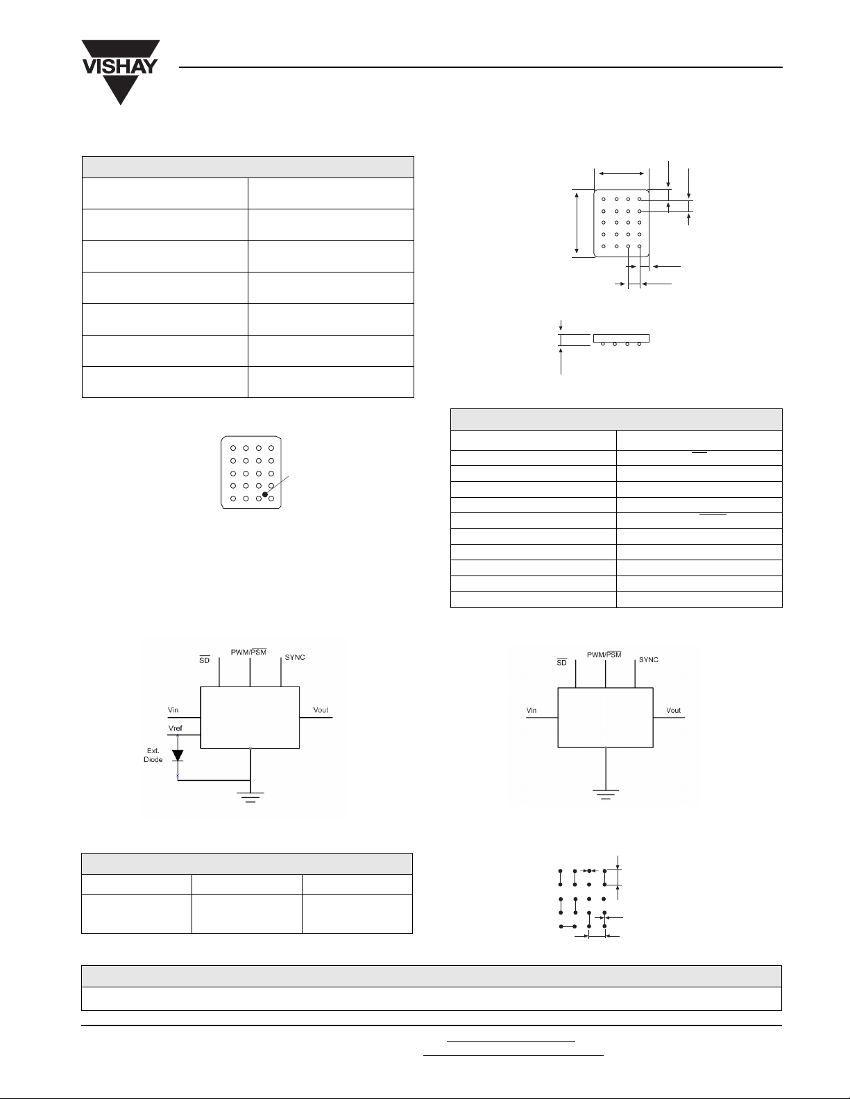
The DC/DC converter is available in 20-ports BGA package.
In order to satisfy the stringent ambient temperature
requirements, the DC/DC converter is designed to handle
the industrial temperature range of - 40°C to + 85°C.
APPLICATION
• Cordless phones, PDAs and others
• Supply voltage source for low-voltage chip sets
• Point of Load (POL) applications such as drivers for
FPGA’s, microprocessors, DSP’s amplifiers, etc.
• Portable computers
• Battery back-up supplies
• Cameras
ORDERING INFORMATION
FX 5545 G008
FUNCTION
SIZE
CIRCUIT IDENTIFIER - G008 or G018
OUTPUT VOLTAGE - Example: 1.2V should be written as 1V2 as the V indicates the decimal point or ADJ
for adjustable version - self selectable output voltage. G018ADJ is only available in the adjustable version
for Vout = 0.9V - 1.3V. For design considerations please see ANF110
PACKAGING - B1 = 10pcs in bulk; B5 = 50pcs in bulk; T1 = 13” reel; T2 = 7” reel.
For lead (Pb)-free solder please add E2 suffix.
www.vishay.com For technical questions, contact Function
22 Revision: 01-Mar-05
For marketing questions, contact FunctionPAK .marketing@vishay.com
PA K@vishay.com
Document Number: 10126
FX5545G008
Vishay
DIMENSIONS in inches [millimeters]
L
W
A
B
C
T
Ball Diameter
BOTTOM SIDE
20
19 18 17
15 14
16
12 11109
876
32
4
*Note: Pin Description application note is available at
www.vishay.com/doc?10119
For adjustable version please refer to Self Selectable Output Voltage
application note which is available at www.vishay.com/doc?10116
**Note: if not used must be connected ti Vin.
***Note: N/C - If the output voltage is 0.9V and higher. For output
voltage of 0.8V connect Vref to MCL4448 (Vishay RF PIN Diode).
0.58 ± 0.01
[14.7 ± 0.25]
0.48 ± 0.01
[12.2 ± 0.25]
0.1 ± 0.01
[2.54 ± 0.25]
0.09 ± 0.01
[2.29 ± 0.25]
0.09 ± 0.01
[2.27 ± 0.25]
0.126 max
[3.2 max]
0.03 ± 0.001
[0.762 ± 0.025]
13
Marked on Upper Side
5
1
W
L
T
PIN CONFIGURATION*
PIN CONNECTION
1, 2 SD
3, 7 SYNC**
4, 8
5, 9 Vin
6, 10 PWM/PSM
11, 12 N/C
13, 17 GND
14, 18 Vout
15, 19 N/C
16, 20 GND
B
A
C
A
Vref***
Pin Configuration for Vo = 0.8V
RECOMMENDED PAD PATTERN
in inches [millimeters]
Pin Configuration for Vo = 0.9V - 4.5V
D
ADF
0.1 ± 0.01
[2.54 ± 0.25]
0.03 ± 0.001
[0.8 ± 0.02]
0.02 ± 0.001
[0.5 ± 0.02]
1
A
A
F
TAPE AND REEL
See Tape and Reel Information - Type B
Document Number: 10126 For technical questions, contact Function
Revision: 01-Mar-05 23
For marketing questions, contact FunctionPAK .marketing@vishay.com
PA K@vishay.com
www.vishay.com

FX5545G008
Vishay
STANDARD ELECTRICAL SPECIFICATIONS
PARAMETER UNIT CONDITION MIN TYP MAX
Input
Voltage Range V
Quiescent Current
Soft Start Time ms T
SD, PWM/PSM
,SYNC
Logic High V V
Logic Low V V
Normal Mode
PSM
Mode µA I
Shutdown Mode
Shutdown Time ms T
Insulation
Te s t Vo l t a ge V
Resistance Ω V
Leakage Current nA V
Output
DC
µA PSM mode 200
µA I
µA I
AC
for Vout = 3.3V 4
SS
T
for Vout = 1.2V 2.6
SS
H
L
DD
DD
DD
for Vout = 3.3V 4
SS
T
for Vout = 1.2V 0.6
SS
60Hz 60sec 750
= 500 V
ISO
ISO
= 500 V
DC
DC
Powe r W 10
Voltage V
Voltage Tolerance %
DC
%
For Vout = 0.9V and above (using external diode BAR065V for
Vout = 0.9V up to 1.3V) at 25°C Ambient Temp.
For Vout = 0.8V up to 1.3V using external diode MCL4448 at
25°C Ambient Temp.
Temp. Coefficient %/°C 0.15
Ripple and Noise mVpp DC to 20 MHz 80
General
Package Weight gr. 1.4
Oscillator
Frequency KHz 400
SYNC Range F
Temperature
SYNC/FOSC
Operation °C - 40 + 85
Storage °C - 55 + 125
Operating Junction Temp. °C T
Thermal Impedance °C/W
* θ
D
j
JA
*Note: WD = Power Dissipated
Rise Time
2.5 6
2.4
11
1 x 10
0.8 to 4.5
- 3 +3
- 5 +5
1.2 1.5
Fall Time
150
82
0.8
750
250
1
5
Rise Time (PWM mode): Vin = 6V; Vout = 3.3V; lout = 3A
Rise Time (PWM mode): Vin = 6V; Vout = 1.2V; lout = 3A
www.vishay.com For technical questions, contact FunctionPAK
24 Revision: 01-Mar-05
For marketing questions, contact FunctionPAK.marketing@vishay.com
Fall Time (PWM mode): Vin = 6V; Vout = 3.3V; lout = 3A
Fall Time (PWM mode): Vin = 6V; Vout = 1.2V; lout = 3A
@vishay.com
Document Number: 10126

PWM MODE
40
50
60
70
80
90
100
0 0.5 2 2.5 3.5
0
10
20
30
1
1.5 3
Vin = 4.0V
Vin = 5.0V
Efficiency (%)
Vout Vs. lout*
Vin = 4.0V
3.5
3.45
3.4
3.35
3.3
3.25
3.2
Vout (V)
3.15
3.1
3.05
3
0.5 1 1.502
lout (A)
2.5 3
3.5
Δ Temp Vs. lout*
Above 25°C Ambient Temperature Vin = 6.0V; Vout = 3.3V
FX5545G008
Vout Vs. Vin*
3.5
3.45
3.4
3.35
3.3
3.25
3.2
3.15
Vout (V)
3.1
3.05
3
373.5 4.5 5.5 6.5
456
Vin (V)
Efficiency Vs. Lout*
Vout = 3.3A
lout = 1A
lout = 2A
lout = 3A
Vishay
60
50
40
30
Temp (°C)
20
D
10
0
0
0.5
1.5 2 2.5
13
3.5
lout (A)
Vout Vs. lout*
Vin = 4.0V
1.5
1.45
1.4
1.35
1.3
1.25
1.2
Vout(V)
1.15
1.1
1.05
1
0.5 1 1.502
lout (A)
2.5 3
3.5
Δ Temp Vs. lout*
Above 25°C Ambient Temperature Vin = 6.0V; Vout = 1.2V
100
95
90
85
80
75
70
Efficiency (%)
65
60
0 0.5 2 2.5 3.5
1.5 3
1
lout (A)
Vout Vs. Vin*
Vin = 6V
1.5
1.45
1.4
1.35
1.3
1.25
1.2
Vout (V)
lout = 2A
1.15
1.1
1.05
1
23 7
lout = 3A
456
Vin (V)
lout = 1A
Efficiency Vs. lout*
Vin = 4.0V; Vout = 1.2V
60
50
40
C)
30
20
Ð Temp (°
Δ Temp (°C)
10
0
* Note: Measurements were taken with Power supply: ZUP 20-40 from Nemic Lambda; Electronic load: 6063B from Agilent; Multimeter Fluke 45
from Fluke and 34401 digital multimeter from Agilent; Scope: Infiniium 54815A from Agilent
Document Number: 10126 For technical questions, contact FunctionPAK
Revision: 01-Mar-05 25
0
13
0.5
1.5 2 2.5
lout (A)
3.5
Iout (A)
@vishay.com www.vishay.com

FX5545G008
Vishay
PSM MODE
Vout Vs. lout*
Vin = 4.0V
3.5
3.45
3.4
3.35
3.3
3.25
3.2
Vout (V)
3.15
3.1
3.05
3.0
0 0.05 0.25
0.1 0.15 0.2
lout (A)
100
90
80
70
60
50
40
Efficiency (%)
30
20
10
0
3.5
3.45
3.4
3.35
3.3
3.25
Vout (V)
3.2
3.15
3.1
3.05
3
Efficiency Vs. lout*
Vin = 4.0V; Vout = 3.3V
0 0.05 0.1 0.2
0.15
Iout (A)
Vout Vs. Vin*
Vin = 6V
lout = 0.1A
lout = 0.15A
3 3.5 6 6.5
4 54.5 5.5
Vin (V)
0.25
Vout Vs. lout*
Vout Vs. Vin*
Vin = 4.0V
1.5
1.45
1.4
1.35
1.3
1.25
1.2
Vout (V)
1.15
1.1
1.05
3.2
0 0.02 0.08 0.12 0.16
0.04 0.06 0.1 0.14
lout (A)
1.5
1.45
1.4
1.35
1.3
1.25
Vout (V)
1.2
1.15
1.1
1.05
lout = 0.15A
1
lout = 0.1A
23 6 7
4 51
Vin (V)
Efficiency Vs. lout*
Vin = 4.0V; Vout = 1.2V
100
90
80
70
60
50
40
Efficiency (%)
30
20
10
0
0 0.02 0.04 0.06 0.08 0.16
Iout (A)
* Note: Measurements were taken with Power supply: ZUP 20-40 from Nemic Lambda; Electronic load: 6063B from Agilent; Multimeter Fluke 45
from Fluke and 34401 digital multimeter from Agilent; Scope: Infiniium 54815A from Agilent
www.vishay.com For technical questions, contact Function
26 Revision: 01-Mar-05
For marketing questions, contact FunctionPAK .marketing@vishay.com
0.140.120.1
PA K@vishay.com
Document Number: 10126

WWW.ALLDATASHEET.COM
Copyright © Each Manufacturing Company.
All Datasheets cannot be modified without permission.
This datasheet has been download from :
www.AllDataSheet.com
100% Free DataSheet Search Site.
Free Download.
No Register.
Fast Search System.
www.AllDataSheet.com
 Loading...