

®
FCSP240LTR
Vishay High Power Products
Chip Scale Package Schottky Barrier Rectifier
FlipKY
PRODUCT SUMMARY
I
F(AV)
V
R
FlipKY
®
FEATURES
• Ultra low VF per footprint area
• Low leakage
• Low thermal resistance
• One-fifth footprint of SMA
RoHS
COMPLIANT
• Super low profile (0.6 mm)
• Available tested on tape and reel
APPLICATIONS
®
• Reverse polarity protection
• Current steering
• Freewheeling
•Flyback
•Oring
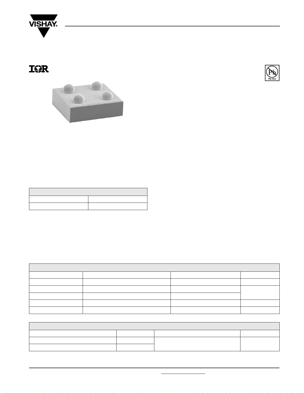
DESCRIPTION
Vishay's FlipKY® product family utilizes wafer level
chip scale packaging to deliver Schottky diodes with the
to PCB footprint area in industry. The four
F
1.5 A
40 V
lowest V
bump 1.5 x 1.5 mm devices can deliver up to 1.5 A and
occupy only 2.3 mm2 of board space. The anode and
cathode connections are made through solder bump pads on
one side of the silicon enabling designers to strategically
place the diodes on the PCB. This design not only minimizes
board space but also reduces thermal resistance and
inductance, which can improve overall circuit efficiency.
Typical applications include hand-held, portable equipment
such as cell phones, MP3 players, bluetooth, GPS, PDAs,
and portable hard disk drives where space savings and
performance are crucial.
MAJOR RATINGS AND CHARACTERISTICS
SYMBOL CHARACTERISTICS MAX. UNITS
V
RRM
I
F(AV)
I
FSM
V
F
T
J
Rectangular waveform 1.5
at 1.5 Apk, TJ = 125 °C 0.42 V
40 V
250
- 55 to 150 °C
A
VOLTAGE RATINGS
PARAMETER SYMBOL FCSP240LTR UNITS
Maximum DC reverse voltage V
Maximum working peak reverse voltage V
Document Number: 94498 For technical questions, contact: diodes-tech@vishay.com
Revision: 23-Aug-07 1
R
RWM
40 V
www.vishay.com
FCSP240LTR
Vishay High Power Products
FlipKY
®
Chip Scale Package
Schottky Barrier Rectifier
ABSOLUTE MAXIMUM RATINGS
PARAMETER SYMBOL TEST CONDITIONS VALUES UNITS
Maximum average forward current I
Maximum peak one cycle
non-repetitive surge current at 25 °C
F(AV)
I
FSM
Non-repetitive avalanche energy E
Repetitive avalanche current I
AR
ELECTRICAL CHARACTERISTICS (TJ = 25 °C unless otherwise specified)
PARAMETER SYMBOL TEST CONDITIONS TYP. MAX. UNITS
Maximum forward
voltage drop
See fig. 1
Maximum reverse
leakage current
See fig. 2
Maximum junction capacitance C
Maximum voltage rate of charge dv/dt Rated V
Note
(1)
Pulse width < 300 µs, duty cycle < 2 %
(1)
V
FM
(1)
I
RM
T
50 % duty cycle at T
5 µs sine or 3 µs rect. pulse
= 97 °C, rectangular waveform 1.5
PCB
Following any rated load
250
condition and with rated
10 ms sine or 6 ms rect. pulse 21
TJ = 25 °C, IAS = 2.0 A, L = 5.0 mH 10 mJ
AS
Current decaying linearly to zero in 1 µs
Frequency limited by T
at 1.5 A
at 3 A 0.55 0.60
at 1.5 A
at 3 A 0.51 0.57
TJ = 25 °C
T
= 125 °C
J
maximum VA = 1.5 x VR typical
J
T
= 25 °C
J
= 125 °C
T
J
V
= Rated V
R
= 20 V 3.5 20
V
R
V
= 10 V 2 10
R
V
= 5 V 1.5 5
R
V
= Rated V
R
= 20 V 3.5 8
V
R
V
= 10 V 2.5 6
R
V
= 5 V 2 5
R
V
RRM
R
R
applied
2.0 A
0.45 0.49
0.37 0.42
15 80
920
VR = 5 VDC (test signal range 100 kHz to 1 MHz) 25 °C - 160 pF
R
- 10 000 V/µs
A
V
µA
mA
THERMAL - MECHANICAL SPECIFICATIONS
PARAMETER SYMBOL TEST CONDITIONS VALUES UNITS
Maximum junction temperature range T
Maximum storage temperature range T
Typical thermal resistance,
junction to PCB
Maximum thermal resistance,
junction to ambient
Notes
dP
(1)
------------dT
(2)
Mounted 1" square PCB
1
tot
J
thermal runaway condition for a diode on its own heatsink
--------------<
R
thJA
www.vishay.com For technical questions, contact: diodes-tech@vishay.com
2 Revision: 23-Aug-07
(1)
J
Stg
(2)
R
thJL
DC operation 40
- 55 to 150 °C
°C/W
R
thJA
62
Document Number: 94498

FCSP240LTR
Chip Scale Package
Schottky Barrier Rectifier
10
1
- Instantaneous
F
I
Forward Current (A)
0.1
0.2 0.4 0.6 0.8 1.0
0
V
- Forward Voltage Drop (V)
FM
Fig. 1 - Maximum Forward Voltage Drop Characteristics
100
10
1
TJ = 150 °C
TJ = 125 °C
TJ = 25 °C
(Per Leg)
TJ = 150 °C
TJ = 125 °C
TJ = 100 °C
1.2
FlipKY
®
Allowable Case Temperature (°C)
Vishay High Power Products
160
150
140
130
120
110
100
90
Square wave (D = 0.50)
80
80 % rated V
70
60
See note (1)
50
0
I
F(AV)
Fig. 4 - Maximum Allowable Case Temperature vs.
Average Forward Current (Per Leg)
1.5
1.0
D = 3/4
D = 1/2
D = 1/3
D = 1/4
D = 1/5
DC
applied
R
1.00.5 1.5 2.0
D = 3/4
D = 1/2
D = 1/3
D = 1/4
D = 1/5
- Average Forward Current (A)
2.5
0.1
- Reverse Current (mA)
0.01
R
I
0.001
0
1051520
V
- Reverse Voltage (V)
R
Fig. 2 - Typical Values of Reverse Current vs.
Reverse Voltage (Per Leg)
1000
TJ = 25 °C
100
- Junction Capacitance (pF)
T
C
10
0
105152025
V
- Reverse Voltage (V)
R
Fig. 3 - Typical Junction Capacitance vs.
Reverse Voltage (Per Leg)
TJ = 75 °C
TJ = 50 °C
TJ = 25 °C
25 30 35
30
0.5
Average Power Loss (W)
0
40
0
I
- Average Forward Current (A)
F(AV)
DC
1.00.5 1.5 2.0
RMS limit
2.5
Fig. 5 - Forward Power Loss Characteristics (Per Leg)
1000
At any rated load condition
and with rated V
following surge
100
RRM
applied
- Non-Repetitive
Surge Current (A)
FSM
I
10
4035
10
100 1000
10 000
tp - Square Wave Pulse Duration (µs)
Fig. 6 - Maximum Non-Repetitive Surge Current (Per Leg)
Note
(1)
Formula used: TC = TJ - (Pd + Pd
Pd = Forward power loss = I
F(AV)
) x R
REV
x VFM at (I
;
thJC
/D) (see fig. 6); Pd
F(AV)
= Inverse power loss = VR1 x IR (1 - D); IR at 80 % VR applied
REV
Document Number: 94498 For technical questions, contact: diodes-tech@vishay.com
www.vishay.com
Revision: 23-Aug-07 3

FCSP240LTR
Vishay High Power Products
D.U.T.
Current
monitor
DIMENSIONS in millimeters (inches)
2 x
0.400
(0.016)
0.10 (0.004)
2 x
B
4
C
1.524
(0.060)
FlipKY
®
Chip Scale Package
Schottky Barrier Rectifier
L
IRFP460
= 25 Ω
R
g
Fig. 7 - Unclamped Inductive Test Circuit
A
3
0.10 (0.004)
High-speed
switch
Freewheel
diode
40HFL40S02
C
2 x
V
= 25 V
d
+
0.600
0.520
0.205
0.175
1
0.800
(0.032)
4 x
Cathode ball 1
Anode ball 4
Recommended footprint
Notes
• Dimensioning and tolerancing per ASME Y14.5M-1994
• Controlling dimension: millimeter
1.524
(0.060)
2
0.800 (0.032)
Ball assignments
1 = Cathode
2 = Cathode
3 = Anode
4 = Anode
Cathode ball 2
Anode ball 3
1.524
0.300
0.395
0.355
0.800 (0.032)
4 x Ø 0.35 (0.014)
www.vishay.com For technical questions, contact: diodes-tech@vishay.com
Document Number: 94498
4 Revision: 23-Aug-07

FCSP240LTR
PART MARKING INFORMATION
Ball 1
location mark
Lot number
TAPE AND REEL INFORMATION
FlipKY
®
Chip Scale Package
Schottky Barrier Rectifier
S
01 123
Vishay High Power Products
Par t number
Workweek (Y, WW)
A1 ball
location
Ø 13"
8 mm
8 mm
4 mm
Conforms to EIA-481 and EIA-541
Document Number: 94498 For technical questions, contact: diodes-tech@vishay.com
Revision: 23-Aug-07 5
Feed direction
www.vishay.com

Legal Disclaimer Notice
Vishay
Notice
The products described herein were acquired by Vishay Intertechnology, Inc., as part of its acquisition of
International Rectifier’s Power Control Systems (PCS) business, which closed in April 2007. Specifications of the
products displayed herein are pending review by Vishay and are subject to the terms and conditions shown below.
Specifications of the products displayed herein are subject to change without notice. Vishay Intertechnology, Inc., or
anyone on its behalf, assumes no responsibility or liability for any errors or inaccuracies.
Information contained herein is intended to provide a product description only. No license, express or implied, by
estoppel or otherwise, to any intellectual property rights is granted by this document. Except as provided in Vishay's
terms and conditions of sale for such products, Vishay assumes no liability whatsoever, and disclaims any express
or implied warranty, relating to sale and/or use of Vishay products including liability or warranties relating to fitness
for a particular purpose, merchantability, or infringement of any patent, copyright, or other intellectual property right.
The products shown herein are not designed for use in medical, life-saving, or life-sustaining applications.
Customers using or selling these products for use in such applications do so at their own risk and agree to fully
indemnify Vishay for any damages resulting from such improper use or sale.
International Rectifier
are registered trademarks of International Rectifier Corporation in the U.S. and other countries. All other product
names noted herein may be trademarks of their respective owners.
®
, IR®, the IR logo, HEXFET®, HEXSense®, HEXDIP®, DOL®, INTERO®, and POWIRTRAIN
®
Document Number: 99901 www.vishay.com
Revision: 12-Mar-07 1
 Loading...