

DG411HS/412HS/413HS
Vishay Siliconix
Precision Monolithic Quad SPST CMOS Analog Switches
DESCRIPTION
The DG411HS series of monolithic quad analog switches
was designed to provide high speed, low error switching of
precision analog signals. Combining low power (0.35 µW)
with high speed (t
suited for portable and battery powered industrial and
military applications.
To achieve high-voltage ratings and superior switching
performance, the DG411HS series was built on Vishay
Siliconix’s high voltage silicon gate process. An epitaxial
layer prevents latchup.
Each switch conducts equally well in both directions when
on, and blocks input voltages up to the supply levels when
off.
The DG411HS and DG412HS respond to opposite control
logic as shown in the Truth Table. The DG413HS has two
normally open and two normally closed switches.
: 68 ns), the DG411HS family is ideally
ON
FEATURES
• 44 V Supply Max Rating
• ± 15 V Analog Signal Range
• On-Resistance - r
• Fast Switching - t
• Ultra Low Power - P
DS(on)
: 68 ns
ON
D
: 25 Ω
: 0.35 µW
• TTL, CMOS Compatible
• Single Supply Capability
BENEFITS
• Widest Dynamic Range
• Low Signal Errors and Distortion
• Break-Before-Make Switching Action
• Simple Interfacing
APPLICATIONS
• Precision Automatic Test Equipment
• Precision Data Acquisition
• Communication Systems
• Battery Powered Systems
• Computer Peripherals
Pb-free
Available
RoHS*
COMPLIANT
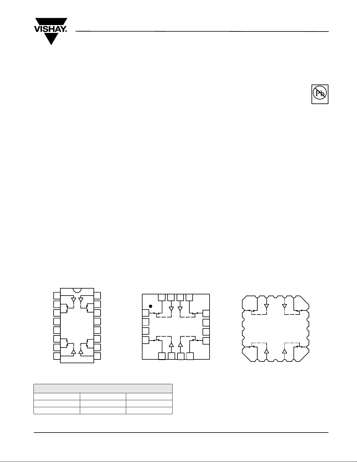
FUNCTIONAL BLOCK DIAGRAM AND PIN CONFIGURATION
DG411HS
QFN16
D1IN
16 15 14 13
5
D4IN
IN2D
1
6
7
IN3D
4
Top View
2
S
12
2
V+
11
V
L
10
S
3
9
8
3
Dual-In-Line and SOIC
IN
1
1
D
2
1
S
3
1
V-
4
5
GND
S
6
4
D
7
4
IN
8
4
DG411HS
Top View
IN
16
2
D
15
2
S
14
2
V+
13
V
12
L
S
11
3
D
10
3
9
IN
3
S
V-
GND
S
1
1
2
3
4
4
TRUTH TABLE
Logic DG411HS DG412HS
0ONOFF
1OFFON
* Pb containing terminations are not RoHS compliant, exemptions may apply
DG411HS
LCC
NC IN2D
D1IN
Key
4
S
1
5
V- V+
6
NC NC
7
GND V
8
S
4
1
1231920
910111213
NC IN
D4IN
4
Top View
2
18
17
16
15
14
3D3
S
2
L
S
3
Document Number: 72053
S-71155-Rev. B, 11-Jun-07
www.vishay.com
1
DG411HS/412HS/413HS
Vishay Siliconix
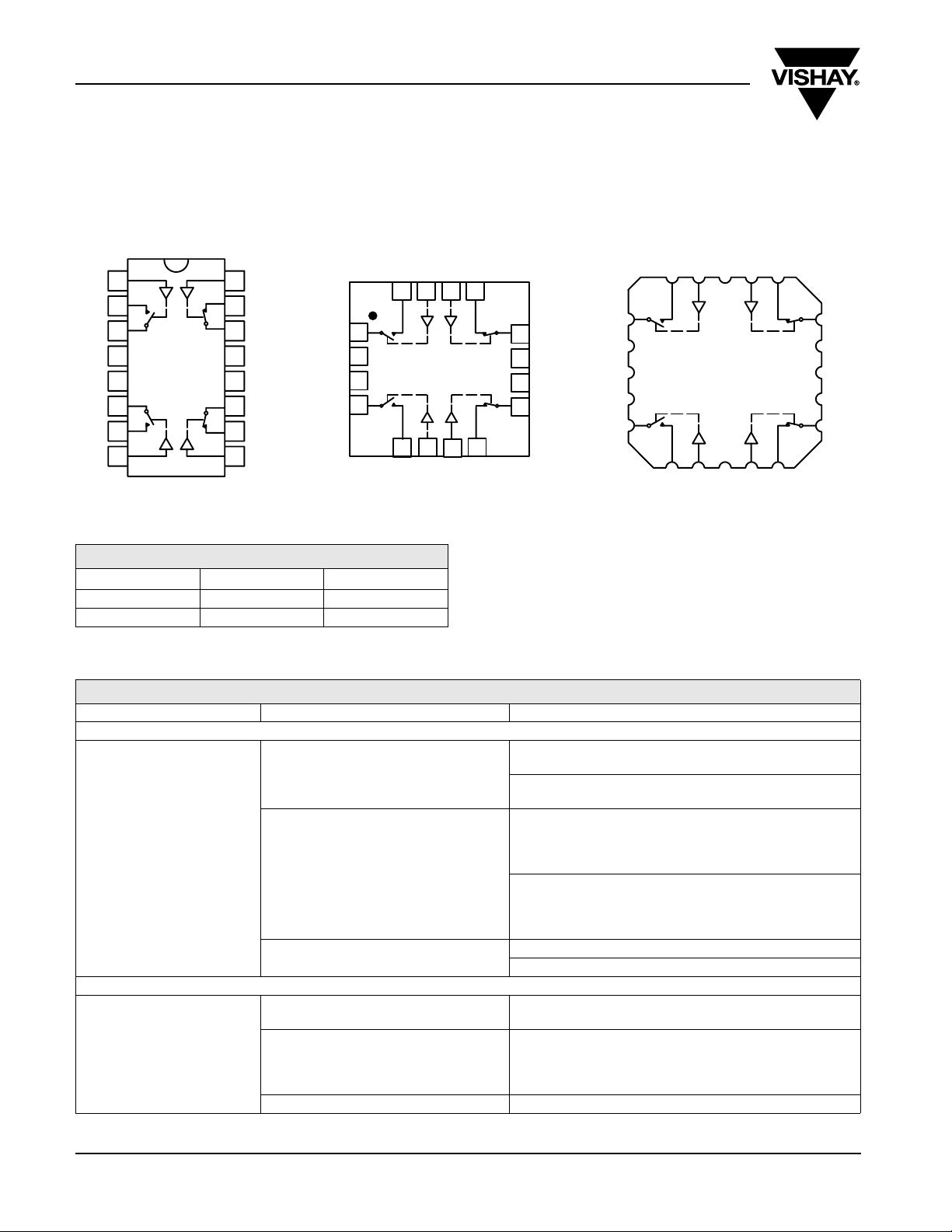
FUNCTIONAL BLOCK DIAGRAM AND PIN CONFIGURATION
DG413HS
Dual-In-Line and SOIC
IN
1
1
D
2
1
3
S
1
V- V+
4
5
GND V
S
6
4
7
D
4
8
IN
4
Top View
16
15
14
13
12
11
10
9
TRUTH TABLE
Logic
0OFFON
1ONOFF
SW
IN
D
2
S
2
L
S
3
D
3
IN
, SW
1
DG413HS
QFN16
IN2D
1
2
3
4
SW2, SW
D1IN
16 15 14 13
6
5
D4IN
Top View
3
2
S
1
V-
GND
S
4
3
4
1
4
7
IN3D
2
S
12
2
V+
11
V
10
L
S
3
9
8
3
Key
4
S
1
5
V- V+
6
NC NC
7
GND V
8
S
4
DG413HS
LCC
D1IN
910111213
D4IN
NC IN2D
1
1231920
NC IN
4
Top View
2
3D3
18
S
2
17
16
15
L
14
S
3
ORDERING INFORMATION
Temp Range Package Part Number
DG411HS/412HS
- 40 to 85 °C
DG413HS
- 40 to 85 °C
DG411HSDJ
16-Pin Plastic DIP
DG411HSDJ-E3
DG412HSDJ
DG412HSDJ-E3
DG411HSDY
DG411HSDY-E3
DG411HSDY-T1
16-Pin Narrow SOIC
DG411HSDY-T1-E3
DG412HSDY
DG412HSDY-E3
DG412HSDY-T1
DG412HSDY-T1-E3
16-Pin QFN 4 x 4 mm
16-Pin Plastic DIP
DG411HSDN-T1-E4
DG412HSDN-T1-E4
DG413HSDJ
DG413HSDJ-E3
DG413HSDY
16-Pin Narrow SOIC
DG413HSDY-E3
DG413HSDY-T1
DG413HSDY-T1-E3
16-Pin QFN 4 x 4 mm DG413HSDN-T1-E4
www.vishay.com
2
Document Number: 72053
S-71155-Rev. B, 11-Jun-07
DG411HS/412HS/413HS
Vishay Siliconix
ABSOLUTE MAXIMUM RATINGS
Parameter Limit Unit
V+ to V- 44
GND to V- 25
V
L
a
Digital Inputs
, VS, V
D
Continuous Current (Any Terminal) 30
Peak Current, S or D (Pulsed 1 ms, 10 % Duty Cycle) 100
Storage Temperature
Power Dissipation (Package)
b
(AK, AZ Suffix) - 65 to 150
(DJ, DY, DN Suffix) - 65 to 125
16-Pin Plastic DIP
16-Pin Narrow SOIC
16-Pin CerDIP
e
LCC-20
16-Pin (4 x 4 mm) QFN
c
d
e
f
Notes:
a. Signals on S
b. All leads welded or soldered to PC Board.
, DX, or INX exceeding V+ or V- will be clamped by internal diodes. Limit forward diode current to maximum current ratings.
X
c. Derate 6 mW/°C above 25 °C.
d. Derate 7.6 mW/°C above 75 °C.
e. Derate 12 mW/°C above 75 °C.
f. Derate 23.5 mW/°C above 70 °C.
(GND - 0.3) to (V+) + 0.3
(V-) - 2 to (V+) + 2
or 30 mA, whichever occurs first
470
600
900
900
1880
V
mA
°C
mW
SPECIFICATIONSa
Test Conditions
Unless Specified
V+ = 15 V, V- = - 15 V
V
Parameter Symbol
Analog Switch
Analog Signal Range
Drain-Source
On-Resistance
Switch Off
Leakage Current
Channel On
Leakage Current
e
V
ANALOG
r
DS(on)
I
S(off)
I
D(off)
I
D(on)
Digital Control
Input Current, V
Input Current, V
Input Capacitance
IN
IN
Low
High
e
I
IL
I
IH
C
IN
Dynamic Characteristics
Tu r n - O n Time
Turn-Off Time
Break-Before-Make
Time Delay
Charge Injection
e
t
t
OFF
ON
t
Q
D
= 5 V, VIN = 2.4 V, 0.8 V
L
V+ = 13.5 V, V- = - 13.5 V
I
= - 10 mA, VD = ± 8.5 V
S
V+ = 16.5 V, V- = - 16.5 V
V
= ± 15.5 mA, VS = ± 15.5 V
D
V+ = 16.5 V, V- = - 16.5 V
V
= VS = ± 15.5 V
D
VIN Under Test = 0.8 V
VIN Under Test = 2.4 V
f = 1 MHz Room 5 pF
RL = 300 Ω, CL = 35 pF
= ± 10 V, See Figure 2
V
S
DG413HS Only, VS = 10 V
R
= 300 Ω, CL = 35 pF
L
= 0 V, Rg = 0 Ω, CL = 10 nF
V
g
f
Tem pb Typ
c
A Suffix
- 55 to 125 °C
d
MaxdMindMax
D Suffix
- 40 to 85 °C
Full - 15 15 - 15 15 V
Room
Full
Room
Full
Room
Full
Room
Full
25 35
± 0.1 - 0.25
- 20
± 0.1 - 0.25
- 20
± 0.1 - 0.4
- 40
45
0.2520- 0.25
- 5
0.2520- 0.25
- 5
0.440- 0.4
- 10
Full 0.005 - 0.5 0.5 - 0.5 0.5
Full 0.005 - 0.5 0.5 - 0.5 0.5
Room
Full
Room
Full
68 105
127
42 80
94
Room 20
Room 22 pC
35
45
0.25
5
0.25
5
0.4
10
105
116
80
90
d
Unit Min
Ω
nA
µA
ns
Document Number: 72053
S-71155-Rev. B, 11-Jun-07
www.vishay.com
3

DG411HS/412HS/413HS
Vishay Siliconix
SPECIFICATIONSa
Test Conditions
Unless Specified
V+ = 15 V, V- = - 15 V
= 5 V, VIN = 2.4 V, 0.8 V
Parameter Symbol
Dynamic Characteristics (Cont’d)
Off Isolation
e
Channel-to-Channel Crosstalk
Source Off Capacitance
Drain Off Capacitance
Channel On Capacitance
e
e
e
OIRR
e
X
TA LK
C
S(off)
C
D(off)
C
D(on)
Power Supplies
Positive Supply Current I+
Negative Supply Current I-
Logic Supply Current
Ground Current
I
GND
V
L
R
= 50 Ω, CL = 5 pF
L
f = 1 MHz
f = 1 MHz
V+ = 16.5 V, V- = - 16.5 V
V
= 0 or 5 V
I
L
IN
f
Tem pb Typ
Room - 91
Room - 88
Room 12
Room 12
Room 30
Room
Full
Room
Full
Room
Full
Room
Full
A Suffix
- 55 to 125 °C
c
d
0.0001 1
- 0.0001 - 1
- 5
0.0001 1
- 0.0001 - 1
- 5
D Suffix
- 40 to 85 °C
MaxdMindMax
5
1
5
- 1
- 5
5
- 1
- 5
1
5
d
Unit Min
dB
pF
µA
SPECIFICATIONSa FOR UNIPOLAR SUPPLIES
Test Conditions
Unless Specified
V+ = 12 V, V- = 0 V
= 5 V, VIN = 2.4 V, 0.8 V
Parameter Symbol
V
L
f
Tem pb Typ
c
A Suffix
- 55 to 125 °C
d
MaxdMindMax
Analog Switch
Analog Signal Range
e
Drain-Source On-Resistance
V
ANALOG
r
DS(on)
V+ = 10.8 V, IS = - 10 mA
= 3 V, 8 V
V
D
Full 12 12 V
Room
Full
49 80
100
Dynamic Characteristics
Tur n-On Ti m e
Turn-Off Time
Break-Before-Make
Time Delay
t
t
OFF
Charge Injection Q
ON
t
Room
RL = 300 Ω, CL = 35 pF
= 8 V, See Figure 2
V
S
D
DG413HS Only, VS = 8 V
= 300 Ω, CL = 35 pF
R
L
= 6 V, Rg = 0 Ω, CL = 1 nF
V
g
Hot
Room
Hot
Room 60
Room 60 pC
95 140
36 70
180
79
Power Supplies
Positive Supply Current I+
Negative Supply Current I-
Logic Supply Current
Ground Current
I
GND
Room
Hot
Room
I
V+ = 13.2 V, V
L
= 0 or 5 V
IN
Hot
Room
Hot
Room
Hot
0.0001 1
- 0.0001 - 1
- 5
0.0001 1
- 0.0001 - 1
- 5
5
5
Notes:
a. Refer to PROCESS OPTION FLOWCHART.
b. Room = 25 °C, Full = as determined by the operating temperature suffix.
c. Typical values are for DESIGN AID ONLY, not guaranteed nor subject to production testing.
d. The algebraic convention whereby the most negative value is a minimum and the most positive a maximum, is used in this data sheet.
e. Guaranteed by design, not subject to production test.
f. V
= input voltage to perform proper function.
IN
Stresses beyond those listed under “Absolute Maximum Ratings” may cause permanent damage to the device. These are stress ratings only, and functional operation
of the device at these or any other conditions beyond those indicated in the operational sections of the specifications is not implied. Exposure to absolute maximum
rating conditions for extended periods may affect device reliability.
D Suffix
- 40 to 85 °C
80
100
140
160
70
74
1
5
- 1
- 5
1
5
- 1
- 5
d
Unit Min
Ω
ns
µA
www.vishay.com
4
Document Number: 72053
S-71155-Rev. B, 11-Jun-07

TYPICAL CHARACTERISTICS 25 °C, unless otherwise noted
65
TA = 25 °C
55
± 5 V
DG411HS/412HS/413HS
Vishay Siliconix
300
250
V+ = 3.0 V
= 3 V
V
L
TA = 25 °C
V
L
= 5 V
(pA)
D
, I
S
I
45
± 8 V
VD - Drain Voltage (V)
± 10 V
- Drain-Source On-Resistance (Ω)
DS(on)
r
35
25
15
5
- 20 - 15 - 10 - 5 0 5 10 15 20
On-Resistance vs. VD and Dual Supply Voltage
50
V+ = + 5 V
V- = - 15 V
25
= 5 V
V
L
0
- 25
- 50
- 75
- 100
- 15 -10 - 5 0 5 10 15
VD or VS - Drain or Source Voltage (V)
I
D(on)
I
S(off)
I
D(off)
Leakage Current vs. Analog Voltage
± 12 V
± 15 V
± 20 V
200
V+ = 5.0 V
V+ = 8.0 V
V+ = 12.0 V
02468101214161820
- Drain Voltage (V)
V
D
- Drain-Source On-Resistance (Ω)
DS(on)
r
150
100
50
0
On-Resistance vs. VD and Unipolar Supply Voltage
45
40
35
30
25
20
15
- Drain-Source On-Resistance (Ω)
10
DS(on)
r
5
- 15 - 10 - 5 0 5 10 15
On-Resistance vs. V
125 °C
85 °C
25 °C
- 55 °C
V
- Drain Voltage (V)
D
and Temperature
D
V+ = 15.0 V
V+ = 20.0 V
V+ = 15 V
V- = - 15 V
= 5 V
V
L
75
65
55
45
35
25
- Drain-Source On-Resistance (Ω)
15
DS(on)
r
5
024681012
On-Resistance vs. V
Document Number: 72053
S-71155-Rev. B, 11-Jun-07
125 °C
°C
85
25 °C
- 55 °C
VD - Drain Voltage (V)
and Temperature
D
V+ = 12 V
V- = 0 V
= 5 V
V
L
0
0- 10
- 20
- 30
(dB)
- 40
- 50
TLAK
- 60
- 70
- 80
LOSS, OIRR, X
- 90
- 100
110
-
100 K 1 M
LOSS
X
TAL K
OIRR
10 M 100 M 1 G
Frequency (Hz)
V+ = 15 V
V- = - 15 V
= 5 V
V
L
= 50 Ω
R
L
Insertion Loss, Off-Isolation, Crosstalk
vs. Frequency
www.vishay.com
5

DG411HS/412HS/413HS
Vishay Siliconix
TYPICAL CHARACTERISTICS 25 °C, unless otherwise noted
100
80
60
40
20
0
- 20
- 40
Q - Charge Injection (pC)
- 60
- 80
- 100
- 15 - 10 - 5 0 5 10 15
V = ± 15 V
V = ± 12 V
Q - Charge Injection (pC)
V - Drain Voltage (V)
Charge Injection vs. Analog Voltage
100
80
60
40
20
0
- 20
- 40
- 60
- 80
- 100
- 15 - 10 - 5 0 5 10 15
V = ± 15 V
V = ± 12 V
VS - Source Voltage (V)
Charge Injection vs. Analog Voltage
(ns)
OFF
T
ON/
T
140
V+ = 15 V
V- = - 15 V
= 5 V
V
120
100
L
80
60
40
20
- 55 - 35 - 15 5 25 45 65 85 105 125
t
ON
t
OFF
Temperature (°C)
Switching Time vs. Temperature
100 mA
10 mA
1 mA
100 µA
V+ = 15 V
V- = - 15 V
V
L
= 5 V
= 1 SW
= 4 SW
I+, I-
(ns)
OFF
T
ON/
T
140
V+ = 12 V
V- = 0 V
V
= 5 V
120
100
80
60
40
20
L
t
ON
t
OFF
- 55 - 35 - 15 5 25 45 65 85 105 125
Temperature (°C)
Switching Time vs. Temperature
www.vishay.com
6
SUPPLY
10 µA
I
1 µA
100 nA
10 nA
100 1 k 10 k 100 k 1 M 10 M
10
f - Frequency (Hz)
I
L
Supply Current vs. Input Switching Frequency
Document Number: 72053
S-71155-Rev. B, 11-Jun-07

SCHEMATIC DIAGRAM (TYPICAL CHANNEL)
V+
V
L
Level
V
IN
Shift/
Drive
DG411HS/412HS/413HS
Vishay Siliconix
S
V-
V+
GND
V-
TEST CIRCUITS
V
L
± 10 V
S D
IN
GND
(includes fixture and stray capacitance)
C
L
VO = V
S
+ 15 V+ 5 V
V+
V-
- 15 V
R
RL + r
L
DS(on)
R
L
300 Ω
C
L
35 pF
Figure 1.
V
O
Figure 2. Switching Time
D
Logic
Input
3 V
50 %
tr < 5 ns
t
< 5 ns
f
0 V
t
OFF
Switch
Input*
V
S
V
O
90 %
0 V
t
ON
Note: Logic input waveform is inverted for switches that
have the opposite logic sense control
90 %
+ 5 V + 15 V
V
L
S
V
S1
V
S2
1
IN
1
S
2
IN
2
GND
CL (includes fixture and stray capacitance)
Document Number: 72053
S-71155-Rev. B, 11-Jun-07
V+
V-
- 15 V
Logic
Input
D
1
V
D
2
R
L2
300 Ω
O2
C
L2
35 pF
R
L1
300 Ω
C
L1
35 pF
V
O1
Switch
Output
Switch
Output
3 V
50 %
0 V
V
S1
V
O1
90 %
0 V
V
S2
V
O2
0 V
90 %
t
D
t
D
Figure 3. Break-Before-Make (DG413HS)
www.vishay.com
7

DG411HS/412HS/413HS
Vishay Siliconix
TEST CIRCUITS
+ 15 V+ 5 V
V
R
g
V
g
L
S
IN
3 V
GND
V+
D
V-
-15 V
V
O
C
L
1 nF
Figure 4. Charge Injection
ΔV
O
V
O
IN
X
IN
X
Q = ΔVO x C
OFFONOFF
OFFONOFF
L
V
S
Rg = 50 Ω
0 V, 2.4 V
X
TALK
C = RF bypass
+ 5 V
+ 15 V
C
V
L
S
IN
GND V-
- 15 V
Off Isolation = 20 log
C = RF Bypass
Figure 6. Off-Isolation
V
S
Rg = 50 Ω
Isolation = 20 log
C
V+
D
C
V
O
V
S
0 V, 2.4 V
0 V, 2.4 V
V
O
V
S
V
O
R
L
50 Ω
+ 5 V
C
V
L
S
1
IN
1
S
NC
2
IN
2
GND V-
Figure 5. Crosstalk
0 V, 2.4 V
+ 15 V
V+
D
D
- 15 V
+ 5 V
C
V
IN
GND V-
C
1
50 Ω
2
V
O
R
L
C
+ 15 V
C
L V+
S
Impedance
D
or Equivalent
C
- 15 V
Figure 7. Source/Drain Capacitances
Meter
HP4192A
Analyzer
Vishay Siliconix maintains worldwide manufacturing capability. Products may be manufactured at one of several qualified locations. Reliability data for Silicon Technology and Package Reliability represent a composite of all qualified locations. For related documents such as package/tape drawings, part marking, and reliability
data, see http://www.vishay.com/ppg?72053.
www.vishay.com
8
Document Number: 72053
S-71155-Rev. B, 11-Jun-07

Legal Disclaimer Notice
Vishay
Disclaimer
All product specifications and data are subject to change without notice.
Vishay Intertechnology, Inc., its affiliates, agents, and employees, and all persons acting on its or their behalf
(collectively, “Vishay”), disclaim any and all liability for any errors, inaccuracies or incompleteness contained herein
or in any other disclosure relating to any product.
Vishay disclaims any and all liability arising out of the use or application of any product described herein or of any
information provided herein to the maximum extent permitted by law. The product specifications do not expand or
otherwise modify Vishay’s terms and conditions of purchase, including but not limited to the warranty expressed
therein, which apply to these products.
No license, express or implied, by estoppel or otherwise, to any intellectual property rights is granted by this
document or by any conduct of Vishay.
The products shown herein are not designed for use in medical, life-saving, or life-sustaining applications unless
otherwise expressly indicated. Customers using or selling Vishay products not expressly indicated for use in such
applications do so entirely at their own risk and agree to fully indemnify Vishay for any damages arising or resulting
from such use or sale. Please contact authorized Vishay personnel to obtain written terms and conditions regarding
products designed for such applications.
Product names and markings noted herein may be trademarks of their respective owners.
Document Number: 91000 www.vishay.com
Revision: 18-Jul-08 1
 Loading...