

DG408L/409L
Vishay Siliconix
Precision 8-Ch/Dual 4-Ch Low Voltage Analog Multiplexers
FEATURES BENEFITS APPLICATIONS
D Pin-For-Pin compatibility with DG408/409
D 2.7- to 12-V Single Supply or
"3- to "6-V Dual Supply Operation
D Lower On-Resistance: r
D Fast Switching: tON - 38 ns, t
DS(on)
- 17 T yp.
- 18 ns
OFF
D High Accuracy
D Single and Dual Power Rail Capacity
D Wide Operating Voltage Range
D Simple Logic Interface
D Break-Before-Make Guaranteed
D Low Leakage: I
- 0.2 nA Max.
S(off)
D Low Charge Injection: 1 pC
D TTL, CMOS, LV Logic (3 V) Compatible
D -82 dB Off-Isolation at 1 MHz
D 2000-V ESD Protection (HBM)
DESCRIPTION
The DG408L/409L are low voltage pin -for -pin compatible
companion devices to the industry standard DG408/409 with
improved performance.
Using BiCMOS wafer fabrication technology allows the
DG408L/409L to operate on single and dual supplies. Single
supply voltage ranges from 3- to 12-V while dual supply
operation is recommended with "3 to "6 V.
The DG408L is an 8-channel single-ended analog multiplexer
D Data Acquisition Systems
D Battery Operated Equipment
D Portable Test Equipment
D Sample and Hold Circuits
D Communication Systems
D SDSL, DSLAM
D Audio and Video Signal Routing
designed to connect one of eight inputs to a common output as
determined by a 3-bit binary address (A
, A1, A2). The DG409L
0
is a dual 4-channel differential analog multiplexer designed to
connect one of four differential inputs to a common dual output
as determined by its 2-bit binary address (A
, A1).
0
Break-before-make switching action to protect against
momentary crosstalk between adjacent channels.
The DG408L/409L provides lower on-resistance, faster
switching time, lower leakage, less power consumption and
higher off-Isolation than the DG408/409.
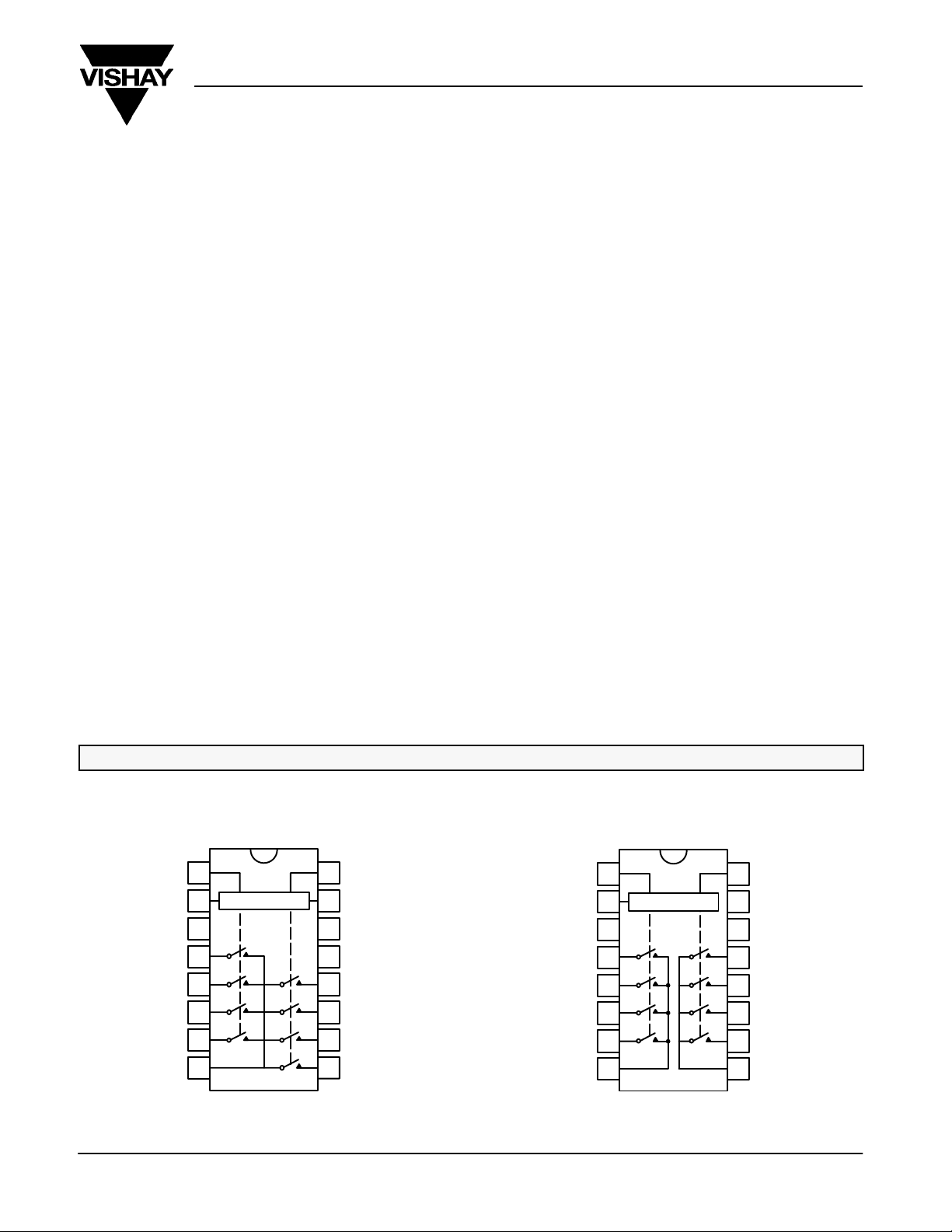
FUNCTIONAL BLOCK DIAGRAMS AND PIN CONFIGURATIONS
DG408L DG409L
Document Number: 71342
S-03720—Rev. D, 07-Apr-03
Dual-In- Line, SOIC and TSSOP
A
0
1
EN
V- GND
S
1
S
2
S
3
S
4
D
Decoders/Drivers
2
3
4
5
6
7
89
Top View
A
1
16
A
2
15
14
V+
13
S
5
12
S
6
11
S
7
10
S
8
A
0
EN GND
V- V+
S
1a
S
2a
S
3a
S
4a
D
a
Dual-In- Line, SOIC and TSSOP
A
1
1
Decoders/Drivers
2
3
4
5
6
7
89
Top View
16
15
14
S
1b
13
S
2b
12
S
3b
11
S
4b
10
D
b
www.vishay.com
1
DG408L/409L
Vishay Siliconix
TRUTH TABLES AND ORDERING INFORMATION
TRUTH TABLE DG408L
A
2
X X X 0 None
0 0 0 1 1
0 0 1 1 2
0 1 0 1 3
0 1 1 1 4
1 0 0 1 5
1 0 1 1 6
1 1 0 1 7
1 1 1 1 8
A
1
A
0
EN On Switch
TRUTH TABLE DG409L
A
1
X X 0 None
0 0 1 1
0 1 1 2
1 0 1 3
1 1 1 4
A
0
Logic “0” = VAL v 0.8 V
“
Logic “1” = VAH w 2.4 V
X = Don’t Care
EN On Switch
”
For low and high voltage levels for VAX and VEN consult “Digital Control” parameters for specific V+ operation.
ORDERING INFORMATION DG408L
Temp Range Package Part Number
_
-40 to 85_C
-55 to 125_C
*Block Diagram and Pin Configuration not shown.
16-Pin SOIC DG408LDY
16-Pin TSSOP DG408LDQ
16-Pin CerDIP
LCC-20* DG408LAZ/883
DG408LAK
DG408LAK/883
ORDERING INFORMATION DG409L
Temp Range Package Part Number
_
-40 to 85_C
-55 to 125_C
*Block Diagram and Pin Configuration not shown.
16-Pin SOIC DG409LDY
16-Pin TSSOP DG409LDQ
16-Pin CerDIP
LCC-20* DG409LAZ/883
DG409LAK
DG409LAK/883
ABSOLUTE MAXIMUM RATINGS
Voltage Referenced to V-
V+ 14 V. . . . . . . . . . . . . . . . . . . . . . . . . . . . . . . . . . . . . . . . . . . . . . . . . . . . . . . . . .
GND 7 V. . . . . . . . . . . . . . . . . . . . . . . . . . . . . . . . . . . . . . . . . . . . . . . . . . . . . . . . .
Digital Inputs
Current (Any Terminal) 30 mA. . . . . . . . . . . . . . . . . . . . . . . . . . . . . . . . . . . . . . .
Peak Current, S or D
(Pulsed at 1 ms, 10% Duty Cycle Max) 100 mA. . . . . . . . . . . . . . . . . . . . . . . .
Storage Temperature: (A Suffix) -65 to 150_C. . . . . . . . . . . . . . . . . . . . . . . . .
www.vishay.com
2
a
, VS, V
D
(D Suffix) -65 to 125_C. . . . . . . . . . . . . . . . . . . . . . . .
(V-) -0.3 V to (V+) +0.3 V. . . . . . . . . . . . . . . . . . . . . .
Power Dissipation (Package)
16-Pin Plastic TSSOP
16-Pin Narrow SOIC
16-Pin CerDIP
LCC-20
Notes
a. Signals on S
internal diodes. Limit forward diode current to maximum current ratings.
b. All leads soldered or welded to PC board.
c. Derate 7.6 mW/_C above 75_C.
d. Derate 12 mW/_C above 75_C.
e. Derate 10 mW/_C above 75_C.
d
e
, D
X
b
c
c
Ax, or EN exceeding V+ or V- will be clamped by
X,
Document Number: 71342
S-03720—Rev. D, 07-Apr-03
650 mW. . . . . . . . . . . . . . . . . . . . . . . . . . . . . . . . . . . .
600 mW. . . . . . . . . . . . . . . . . . . . . . . . . . . . . . . . . . . . . .
900 mW. . . . . . . . . . . . . . . . . . . . . . . . . . . . . . . . . . . . . . . . . . .
750 mW. . . . . . . . . . . . . . . . . . . . . . . . . . . . . . . . . . . . . . . . . . . . . . . . .
SPECIFICATIONS (SINGLE SUPPLY 12 V)
VD = 10.8 V, VD = 2 V or 9 V, IS = 10 mA
VEN = 0 V, VD = 11 V or 1 V
V
ns
F
DG408L/409L
Vishay Siliconix
Parameter Symbol
T est Conditions
Unless Otherwise Specified
V+ = 12 V, "10%, V- = 0 V
V
= 0.8 V or 2.4 V
EN
f
TempbTyp
A Suffix
-55 to 125_C
d
MincMaxcMincMax
D Suffix
-40 to 85_C
c
Unit
Analog Switch
Analog Signal Range
Drain-Source On-Resistance r
r
Matching
DS(on)
Between Channels
On-Resistance Flatness
Switch Off Leakage Current
Channel On Leakage Current I
e
g
i
V
ANALOG
DS(on)
r
r
FLAT(on)
I
S(off)
I
D(off)
D(on)
Full 0 12 0 12 V
VD = 10.8 V, VD = 2 V or 9 V, IS = 10 mA
Sequence Each Switch On
DS
VD = 10.8 V, VD = 2 V or 9 V, IS = 10 mA
Room
Full
17 29
38
Room 1 3 3
29
35
Room 3 7 7
VEN = 0 V, VD = 11 V or 1 V
V
= 1 V or 11 V
S
V
= VD = 1 V or 11 V
S
Room
Full
Room
Full
Room
Full
-1
-15115-1-10110
-1
-15115-1-10110
-1
-15115-1-10110
nA
Digital Control
Logic High Input Voltage V
Logic Low Input Voltage V
Input Current I
INH
INL
IN
VAX = VEN = 2.4 V or 0.8 V Full -1.5 1.5 -1 1 A
Full 2.4 2.4
Full 0.8 0.8
Dynamic Characteristics
Transition Time t
Break-Before-Make Time t
Enable Turn-On Time t
Enable Turn-Off Time t
Charge Injection
Off Isolation
Crosstalk
Source Off Capacitance
Drain Off Capacitance
Drain On Capacitance
e
e, h
e
e
e
e
VS1 = 8 V, VS8 = 0 V, (DG408L)
TRANS
OPEN
ON(EN)
OFF(EN)
V
S1b
V
S(all)
VAX = 0 V, VS1 = 5 V (DG408L)
VAX = 0 V, V
Q CL = 1 nF, V
OIRR
X
TALK
C
C
C
S(off)
D(off)
D(on)
f = 1 MHz, VS = 0 V, VEN = 0 V Room 7
f = 1 MHz, VD = 2.4 V, VEN = 0 V Room 20
f = 1 MHz, VD = 0 V, VEN = 2.4 V
= 8 V, V
= 0 V, (DG409L)
S4b
See Figure 2
= VDA = 5 V, See Figure 4
= 5 V (DG409L)
S1b
See Figure 3
= 0 V, R
GEN
GEN
f = 100 kHz, RL = 1 k
(DG409L only)
= 0 Room 1 5 5 pC
Room
Full
Room
Full
Room
Full
Room
Full
30 60
11 1 1
38 55
18 25
Room -70
Room -82
Room 31
68
60
65
ns
60
35
55
60
25
30
dB
p
Power Supplies
Power Supply Range V+ 3 12 3 12 V
Power Supply Current I+ VEN = VA = 0 V or 5 V Room 0.2 0.7 0.7 mA
Document Number: 71342
S-03720—Rev. D, 07-Apr-03
www.vishay.com
3
DG408L/409L
V+ = 5.5 V, V- = 5.5 V
V
ns
pF
Vishay Siliconix
SPECIFICATIONS (DUAL SUPPLY V+ = 5 V, V = 5 V)
Parameter Symbol
Analog Switch
Analog Signal Range
Drain-Source On-Resistance r
Switch Off Leakage Current
Channel On Leakage
a
Current
e
V
a
Digital Control
Logic High Input Voltage V
Logic Low Input Voltage V
Input Current
a
Dynamic Characteristics
Transition Time
Break-Before-Make Time
Enable Turn-On Time
Enable Turn-Off Time
Source Off Capacitance
Drain Off Capacitance
Drain On Capacitance
e
e
e
e
e
e
e
t
t
t
OFF(EN)
ANALOG
DS(on)
I
S(off)
I
D(off)
I
D(on)
INH
INL
I
IN
TRANS
t
OPEN
ON(EN)
C
S(off)
C
D(off)
C
D(on)
T est Conditions
Unless Otherwise Specified
V+ = 5 V, V- = -5 V "10%, V- = 0 V
V
= 0.6 V or 2.4 V
EN
f
TempbTyp
A Suffix
-55 to 125_C
d
MincMaxcMincMax
-40 to 85_C
D Suffix
Full -5 5 -5 5 V
VD = "3.5 V, IS = 10 mA
Sequence Each Switch On
V+ = 5.5 V, V- = 5.5 V
VEN = 0 V, VD = "4.5 V, VS = #4.5 V
V+ = 5.5 V, V- = 5.5 V
V
= 2.4 V, VD = "4.5 V, VS = #4.5 V
EN
Room
Full
Room
Full
Room
Full
Room
Full
20 40
-15115
-15115
-15115
50
-1
-1
-1
-1
-10110
-1
-10110
-1
-10110
Full 2.4 2.4
Full 0.6 0.6
VAX = VEN = 2.4 V or 0.6 V Full -1.5 1.5 -1 1 A
VS1 = 3.5 V, VS8 = -3.5 V, (DG408L)
V
= 3.5 V, V
S1b
V
= VDA = 3.5 V, See Figure 4
S(all)
VAX = 0 V, VS1 = 3.5 V (DG408L)
VAX = 0 V, V
= -3.5 V, (DG409L)
S4b
See Figure 2
= 3.5 V (DG409L)
S1b
See Figure 3
Room
Full
Room
Full
Room
Full
Room
Full
30 60
78
8 1 1
25 55
20 40
68
50
f = 1 MHz, VS = 0 V, VEN = 0 V Room 6
f = 1 MHz, VD = 0 V, VEN = 0 V Room 15
f = 1 MHz, VD = 0 V, VEN = 2.4 V Room 29
c
Unit
40
50
nA
60
65
ns
55
60
40
45
pF
www.vishay.com
4
Document Number: 71342
S-03720—Rev. D, 07-Apr-03

SPECIFICATIONS (SINGLE SUPPLY 5 V)
V+ = 4.5 V, VD = 1 V or 3.5 V, IS = 5 mA
V+ = 5.5 V, VS = 1 V or 4 V
V+ = 5 V
V
ns
F
T est Conditions
Unless Otherwise Specified
Parameter Symbol
Analog Switch
Analog Signal Range
Drain-Source On-Resistance r
r
Matching
DS(on)
Between Channels
On-Resistance Flatness
Switch Off Leakage Current
Channel On Leakage Current
e
g
i
V
r
FLAT(on)
a
a
Digital Control
Logic High Input Voltage V
Logic Low Input Voltage V
Input Current
a
Dynamic Characteristics
Transition Time
Break-Before-Make Time
Enable Turn-On Time
Enable Turn-Off Time
Charge Injection
Off Isolatione,
Crosstalk
Source Off Capacitance
Drain Off Capacitance
Drain On Capacitance
e
e
e
e
e
h
e
e
e
e
t
t
t
OFF(EN)
ANALOG
DS(on)
r
DS
I
S(off)
I
D(off)
I
D(on)
INH
INL
I
IN
TRANS
t
OPEN
ON(EN)
Q CL = 1 nF, R
OIRR
X
TALK
C
S(off)
C
D(off)
C
D(on)
V+ = 5 V, "10%, V- = 0 V
= 0.6 V or 2.4 V
V
EN
V+ = 4.5 V, VD or VS = 1 V or 3.5 V, ID =
V+ = 4.5 V, VD = 1 V or 3.5 V, IS = 5 mA
V+ = 5.5 V, VS = 1 V or 4 V
VD = 4 V or 1 V
V+ = 5.5 V, VD = VS = 1 V or 4 V
Sequence Each Switch On
VAX = VEN = 2.4 V or 0.6 V Full -1.5 1.5 -1 1 A
VS1 = 3.5 V, VS8 = 0 V, (DG408L)
V
= 3.5 V, V
S1b
V
VAX = 0 V, VS1 = 3.5 V (DG408L)
VAX = 0 V, V
See Figure 2
= VDA = 3.5 V, See Figure 4
S(all)
S1b
See Figure 3
GEN
RL = 1 k f = 100 kHz
f = 1 MHz, VS = 0 V, VEN = 0 V Room 8
f = 1 MHz, VD = 0 V, VEN = 0 V Room 21
f = 1 MHz, VD = 0 V, VEN = 2.4 V
(DG409L only)
f
5 mA
= 0 V, (DG409L)
S4b
= 3.5 V (DG409L)
= 0 , V
= 0 V Room 1 5 5 pC
GEN
DG408L/409L
Vishay Siliconix
A Suffix
-55 to 125_C
b
Temp
Full 0 5 0 5 V
Room
Full
Room 1.5 3 3
Room 4 4
Room
Full
Room
Full
Room
Full
Full 2.4 2.4
Full 0.6 0.6
Room
Full
Room
Full
Room
Full
Room
Full
Room -70
Room -80
Room 32
d
Typ
MincMaxcMincMaxcUnit
35 49
-15115-1-10110
-15115-1-10110
-15115-1-10110
44 125
62
-1
-1
-1
138
17 1 1
43 60
26 45
70
60
D Suffix
-40 to 85_C
125
135
40
62
60
65
45
50
nA
ns
dB
p
Document Number: 71342
S-03720—Rev. D, 07-Apr-03
www.vishay.com
5

DG408L/409L
V
ns
F
Vishay Siliconix
SPECIFICATIONS (SINGLE SUPPLY 3 V)
T est Conditions
Unless Otherwise Specified
Parameter Symbol
V+ = 3 V, "10%, V- = 0 V
= 0.4 V or 2.0 V
V
EN
f
Temp
b
Typ
Analog Switch
Analog Signal Range
Drain-Source On-Resistance r
Switch Off Leakage Current
Channel On Leakage Current
e
V
ANALOG
DS(on)
I
S(off)
a
I
D(off)
a
I
D(on)
V+ = 2.7 V, VD = 0.5 or 2.2 V, IS = 5 mA
V+ = 3.3 V, VS = 2 or 1 V, VD = 1 or 2 V
V+ = 3.3 V, VD = VS = 1 or 2 V
Sequence Each Switch On
Full 0 3 0 3 V
Room
Full
Room
Full
Room
Full
Room
Full
60 80
Digital Control
Logic High Input Voltage V
Logic Low Input Voltage V
Input Current
a
I
INH
INL
IN
VAX = VEN = 2.4 V or 0.4 V Full -1.5 1.5 -1 1 A
Full 2 2
Full 0.4 0.4
Dynamic Characteristics
VS1 = 1.5 V, VS8 = 0 V, (DG408L)
Transition Time t
Break-Before-Make Time t
Enable Turn-On Time t
Enable Turn-Off Time t
Charge Injection
Off Isolation
Crosstalk
Source Off Capacitance
Drain Off Capacitance
Drain On Capacitance
Notes
a. Leakage parameters are guaranteed by worst case test condition and not subject to production test.
b. Room = 25_C, Full = as determined by the operating temperature suffix.
c. The algebraic convention whereby the most negative value is a minimum and the most positive a maximum, is used in this data sheet.
d. Typical values are for DESIGN AID ONLY, not guaranteed nor subject to production testing.
e. Guaranteed by design, not subject to production test.
f. V
IN
g. r
DS(on)
h. Worst case isolation occurs on Channel 4 do to proximity to the drain pin.
i. r
DS(on)
e
e, h
e
e
e
e
= input voltage to perform proper function.
= r
Max - r
DS(on)
flatness is measured as the difference between the minimum and maximum measured values across a defined Analog signal.
DS(on)
TRANS
OPEN
ON(EN)
OFF(EN)
Q CL = 1 nF, R
OIRR
X
TALK
C
S(off)
C
D(off)
C
D(on)
Min.
V
= 1.5 V, V
S1b
V
= VDA = 1.5 V, See Figure 4
S(all)
VAX = 0 V, VS1 = 1.5 V (DG408L)
VAX = 0 V, V
= 0 V, (DG409L)
S4b
See Figure 2
= 1.5 V (DG409L)
S1b
See Figure 3
= 0 , V
GEN
= 0 V Room 0.4 5 5 pC
GEN
f = 100 kHz, RL = 1 k
f = 1 MHz, VS = 0 V, VEN = 0 V Room 8
f = 1 MHz, VD = 0 V, VEN = 0 V Room 19
f = 1 MHz, VD = 0 V, VEN = 2 V
(DG409L only)
Room
Full
Room
Full
Room
Full
Room
Full
75 150
32 1 1
70 95
55 100
Room -70
Room -79
Room 33
A Suffix
-55 to 125_C
d
MincMaxcMincMaxcUnit
105
-1
-15115
-1
-15115
-1
-15115
175
115
115
D Suffix
-40 to 85_C
100
-1
-10110
-1
-10110
-1
-10110
150
175
105
100
105
80
nA
ns
95
dB
p
www.vishay.com
6
Document Number: 71342
S-03720—Rev. D, 07-Apr-03

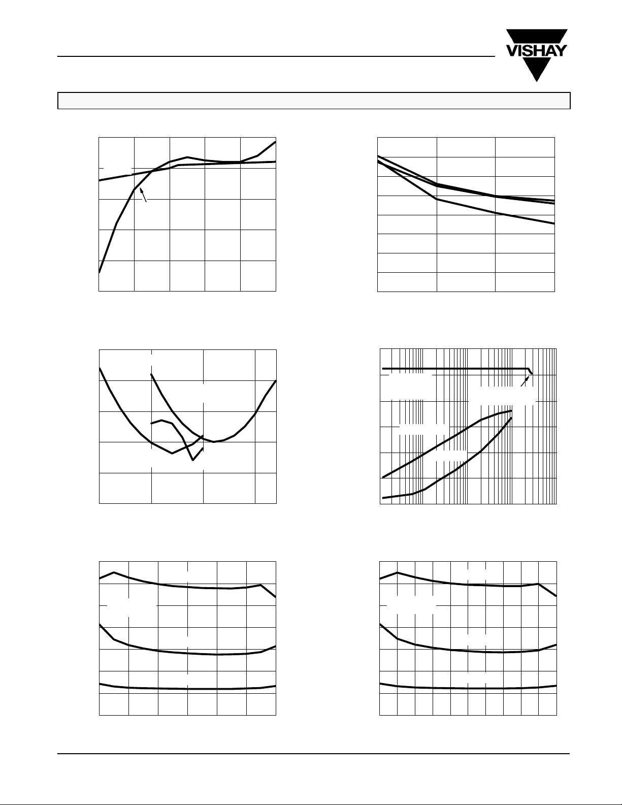
TYPICAL CHARACTERISTICS (25_C UNLESS NOTED)
r
vs. VD and Power Supply
DS(on)
V+ = 2.7 V
V+ = 4.5 V
V+ = 12 V
- Drain-Source On-Resistnace ()
DS9on)
r
- Drain-Source On-Resistnace ()
DS9on)
r
80
70
60
50
40
30
20
10
0
024681012
DG408L/409L
Vishay Siliconix
r
vs. VD and Power Supply
25
20
15
10
5
0
-5 -3 -1 1 3 5
DS(on)
V+ = 5 V
V- = -5 V
(V)
T
V
VD - Drain Voltage (V)
Input Threshold vs. V+ Supply Voltage
1.8
1.6
1.4
1.2
1.0
0.8
0.6
0.4
0.2
0.0
35
30
25
Upper Threshold Limit
Low Threshold Limit
0 2 4 6 8 10 12 14
V+ - Positive Supply Voltage (V)
r
vs. VD and Temperature
DS(on)
85_C
125_C
- Drain-Source On-Resistnace ()
DS9on)
r
VD - Drain Voltage (V)
r
vs. VD and Temperature
50
40
30
20
10
0
0123456
DS(on)
85_C
125_C
25_C
-55_C
VD - Drain Voltage (V)
Switching Time vs. Positive Supply V oltage
70
60
50
20
15
10
- Drain-Source On-Resistnace ()
5
DS9on)
r
0
-6 -4 -2 0 2 4 6
Document Number: 71342
S-03720—Rev. D, 07-Apr-03
25_C
-55_C
VD - Drain Voltage (V)
40
30
Switching Speed (nS)
20
10
0
0 2 4 6 8 10 12 14
t
TRANS
t
ON
t
OFF
V+ - Positive Supply Voltage (V)
www.vishay.com
7
DG408L/409L
Vishay Siliconix
TYPICAL CHARACTERISTICS (25_C UNLESS NOTED)
10
0
I
S(off)
-10
-20
Leakage Current (pA)Q - Charge Injection (pC)
-30
-40
-5 -3 -1 1 3 5
Charge Injection vs. Analog Voltage
1.0
CL = 1000 pF
0.8
0.6
0.4
V+ = 5 V
V- = -5 V
0.2
Leakage Current vs. Analog Voltage
I
D(off)
I
D(on)
VD, VS - Analog V oltage (V)
V+ = 12 V
V- = 0 V
V+ = 5 V
V- = 0 V
40
35
30
25
20
15
Switching Speed (nS)
10
5
0
3456
Insertion Loss, Off Isolation and Crosstalk
10
-10
V+ = 3 V
V- = 0 V
R
-30
-50
Loss (dB)
-70
-90
Switching Time vs.
Dual Power Supply Voltage
" - Dual Power Supply Voltage (V)
vs. Frequency (Single Supply)
= 50
L
Off Isolation
Crosstalk
Insertion Loss
-3 dB = 280 MHz
t
OFF
t
ON
t
TRANS
0.0
-5 0 5 10
Drain/Source Capacitance vs. Analog Voltage
35
30
V+ = 12 V
25
V- = 0 V
20
15
10
- Drain/Source Capacitance (pF)
S
, C
D
5
C
0
024681012
www.vishay.com
8
VS - Source Voltage (V)
C
D(on)
C
D(off)
C
S(off)
-110
0.1
1
Drain/Source Capacitance vs. Analog Voltage
35
30
V+ = 5 V
25
V- = -5 V
20
15
10
- Drain/Source Capacitance (pF)
S
, C
D
C
5
0
-5 -4 -3 -2 -1 0 1 2 3 4 5
10
Frequency (MHz)
C
D(on)
C
D(off)
C
S(off)
Document Number: 71342
S-03720—Rev. D, 07-Apr-03
100 1000
SCHEMATIC DIAGRAM (TYPICAL CHANNEL)
V+
GND
A
0
DG408L/409L
Vishay Siliconix
D
A
X
EN
V-
TEST CIRCUITS
A
A
50
3 V
50
3 V
A
EN
A
A
EN
2
1
0
1
0
DG408L
DG409L
V+
V+
V+
S2 - S
V-GND
V-
V+
S1a - S4a, D
V+
V-GND
V-
V+
Level
Shift
Decode/
Drive
V-
S
1
S
n
FIGURE 1.
S
7
S
D
S
1b
a
S
4b
D
b
1
8
300
300
V
S1
V
S8
V
O
35 pF
V
S1
V
SB4
V
O
Logic
Input
V
Switch
Output
35 pF
3 V
50%
0 V
AX
V
S1
V
50%
O
V
S8
t
TRANS
S
ON
1
90%
S
ON (DG408L)
8
or
S
ON (DG409L)
4
tr <20 ns
t
<20 ns
f
90%
t
TRANS
Document Number: 71342
S-03720—Rev. D, 07-Apr-03
FIGURE 2. Transition Time
www.vishay.com
9

DG408L/409L
Vishay Siliconix
TEST CIRCUITS
V+
50
50
V+
EN
A
0
DG408L
A
1
A
2
GND V-
V+
V+
EN
A
0
A
1
S1a - S4a, D
DG409L
GND V-
S2 - S
V-
S2b - S
V-
S
S
300
1b
a
4b
D
b
300
V
1
8
D
S1
3 V
0 V
t
ON(EN)
50%
35 pF
V
O
Logic
Input
0 V
Switch
Output
V
V
S1
V
O
O
V
O
90%
tr <20 ns
t
<20 ns
f
10%
t
OFF(EN)
35 pF
FIGURE 3. Enable Switching Time
3 V
www.vishay.com
10
50
EN
A
A
A
0
1
2
V+
All S and D
DG408L
DG409L
GND V-
Db, D
V-
bbm.5
4/9
V
a
300
S1
V
O
35 pF
FIGURE 4. Break-Before-Make Interval
Logic
Input
Switch
Output
V
O
3 V
0 V
0 V
tr <20 ns
t
<20 ns
f
50%
V
S
80%
t
OPEN
Document Number: 71342
S-03720—Rev. D, 07-Apr-03

TEST CIRCUITS
R
g
V
g
Channel
Select
V+
V+
S
X
EN
A
0
A
1
A
2
GND V-
V+
C
L
1 nF
V
D
V-
FIGURE 5. Charge Injection
DG408L/409L
Vishay Siliconix
3 V
Logic
Input
O
Switch
Output
OFF ON
OFF
0 V
VO is the measured voltage due to charge transfer
error Q, when the channel turns off.
Q = C
x V
L
O
V+
V
O
V
S
V
S
Rg = 50
Rg = 50
V
V
IN
S
X
S
8
A
0
A
1
A
2
V+
EN
GND V-
D
V
O
Rg = 50
R
L
1 k
IN
S
1
S
V
S
X
S
8
A
0
A
1
A
2
GND V-
V-
V
Off Isolation = 20 log
OUT
V
IN
FIGURE 6. Off Isolation FIGURE 7. Crosstalk
V+V+
S
1
A
0
A
1
A
2
GND V-EN
V+
A
D
Channel
V
O
Select
A
A
R
L
1 k
2
1
0
GND
V+
EN
V-
S
1
S
8
D
V+
D
EN
V-
Crosstalk = 20 log
R
1 k
V
Meter
HP4192A
Impedance
Analyzer
or Equivalent
f = 1 MHz
OUT
V
V
O
L
IN
Document Number: 71342
S-03720—Rev. D, 07-Apr-03
V-
Insertion Loss = 20 log
FIGURE 8. Insertion Loss
V
OUT
V
V-
IN
FIGURE 9. Source Drain Capacitance
www.vishay.com
11
 Loading...