

Page 1
DG408/409
Vishay Siliconix
8-Ch/Dual 4-Ch High-Performance CMOS Analog Multiplexers
FEATURES BENEFITS APPLICATIONS
D Low On-Resistance—r
DS(on)
: 100
D Low Charge Injection—Q: 20 pC
D Fast Transition Time—t
D Low Power—I
SUPPLY
: 10 A
TRANS
: 160 ns
D Single Supply Capability
D 44-V Supply Max Rating
D Reduced Switching Errors
D Reduced Glitching
D Improved Data Throughput
D Reduced Power Consumption
D Increased Ruggedness
D Wide Supply Ranges ("5 V to "20 V)
D TTL Compatible Logic
DESCRIPTION
The DG408 is an 8-channel single-ended analog multiplexer
designed to connect one of eight inputs to a common output
as determined by a 3-bit binary address (A0, A1, A2). The
DG409 is a dual 4-channel differential analog multiplexer
designed to connect one of four differential inputs to a common
dual output as determined by its 2-bit binary address (A0, A1).
Break-before-make switching action protects against
momentary crosstalk between adjacent channels.
An on channel conducts current equally well in both directions.
In the off state each channel blocks voltages up to the power
supply rails. An enable (EN) function allows the user to reset
the multiplexer/demultiplexer to all switches off for stacking
several devices. All control inputs, address (A
(EN) are TTL compatible over the full specified operating
temperature range.
) and enable
x
D Data Acquisition Systems
D Audio Signal Routing
D ATE Systems
D Battery Powered Systems
D High Rel Systems
D Single Supply Systems
D Medical Instrumentation
Applications for the DG408/409 include high speed data
acquisition, audio signal switching and routing, ATE systems,
and avionics. High performance and low power dissipation
make them ideal for battery operated and remote
instrumentation applications.
Designed in the 44-V silicon-gate CMOS process, the
absolute maximum voltage rating is extended to 44 V.
Additionally, single supply operation is also allowed. An
epitaxial layer prevents latchup.
For additional information please see Technical Article T A201
(FaxBack Number 70600).
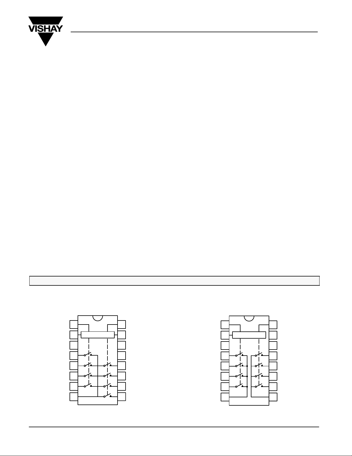
FUNCTIONAL BLOCK DIAGRAM AND PIN CONFIGURATION
DG408 DG409
A
0
EN
V- GND
S
1
S
2
S
3
S
4
D
Document Number: 70062
S-03081—Rev. F, 27-Jan-03
Dual-In-Line
SOIC and TSSOP
A
1
Decoders/Drivers
2
3
4
5
6
7
89
Top View
1
16
A
2
15
14
V+
13
S
5
12
S
6
11
S
7
10
S
8
Dual-In-Line
SOIC and TSSOP
A
0
1
EN GND
V- V+
S
1a
S
2a
S
3a
S
4a
D
a
Decoders/Drivers
2
3
4
5
6
7
89
Top View
A
1
16
15
14
S
1b
13
S
2b
12
S
3b
11
S
4b
10
D
b
www.vishay.com
1
Page 2
DG408/409
Vishay Siliconix
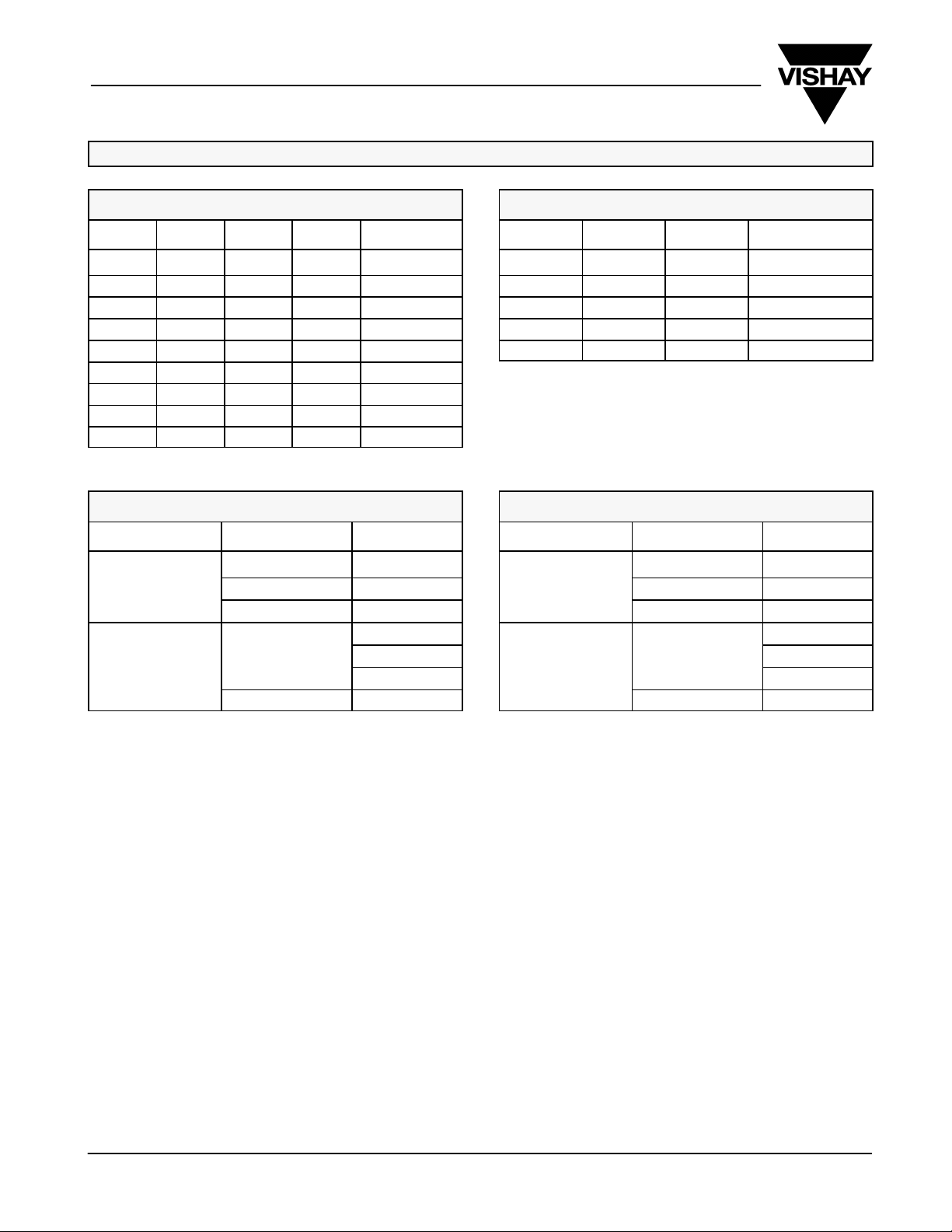
TRUTH TABLES AND ORDERING INFORMATION
TRUTH TABLE DG408
A
2
X X X 0 None
0 0 0 1 1
0 0 1 1 2
0 1 0 1 3
0 1 1 1 4
1 0 0 1 5
1 0 1 1 6
1 1 0 1 7
1 1 1 1 8
A
1
A
0
EN On Switch
ORDERING INFORMATION DG408
Temp Range Package Part Number
16-Pin Plastic DIP DG408DJ
-40 to 85_C
-55 to 125_C
*Block Diagram and Pin Configuration not shown.
_
16-Pin SOIC DG408DY
16-Pin TSSOP DG408DQ
DG408AK
16-Pin CerDIP
LCC-20* 5962-9204201M2A
DG408AK/883
5962-9204201MEA
TRUTH TABLE DG409
A
1
X X 0 None
0 0 1 1
0 1 1 2
1 0 1 3
1 1 1 4
A
0
Logic “0” =VAL v 0.8 V
Logic “1” =VAH w 2.4 V
X = Don’t Care
EN On Switch
ORDERING INFORMATION DG409
Temp Range Package Part Number
16-Pin Plastic DIP DG409DJ
-40 to 85_C
-55 to 125_C
_
16-Pin SOIC DG409DY
16-Pin TSSOP DG409DQ
DG409AK
16-Pin CerDIP
LCC-20* 5962-9204202M2A
DG409AK/883
5962-9204202MEA
ABSOLUTE MAXIMUM RATINGS
Voltage Referenced to V-
V+ 44 V. . . . . . . . . . . . . . . . . . . . . . . . . . . . . . . . . . . . . . . . . . . . . . . . . . . . . . . . . . .
GND 25 V. . . . . . . . . . . . . . . . . . . . . . . . . . . . . . . . . . . . . . . . . . . . . . . . . . . . . . . . . .
Digital Inputs
20 mA, whichever occurs first
Current (Any Terminal) 30 mA. . . . . . . . . . . . . . . . . . . . . . . . . . . . . . . . . . . . . . . .
Peak Current, S or D
(Pulsed at 1 ms, 10% Duty Cycle Max) 100 mA. . . . . . . . . . . . . . . . . . . . . . . . .
Storage Temperature (AK Suffix) -65 to 150_C. . . . . . . . . . . . . . . . . . .
Power Dissipation (Package)
16-Pin Plastic DIP
www.vishay.com
2
a
, VS, V
D
(DJ, DY Suffix) -65 to 125_C. . . . . . . . . . . . . . .
c
b
(V-) -2 V to (V+) +2 V or. . . . . . . . . . . . . . . . . . . . . . . .
450 mW. . . . . . . . . . . . . . . . . . . . . . . . . . . . . . . . . . . . . . . . .
16-Pin Narrow SOIC and TSSOP
16-Pin CerDIP
LCC-20
Notes
a. Signals on S
diodes. Limit forward diode current to maximum current ratings.
b. All leads soldered or welded to PC board.
c. Derate 6 mW/_C above 75_C.
d. Derate 7.6 mW/_C above 75_C.
e. Derate 12 mW/_C above 75_C.
f. Derate 10 mW/_C above 75_C.
e
f
, DX or INX exceeding V+ or V- will be clamped by internal
X
d
Document Number: 70062
S-03081—Rev. F, 27-Jan-03
600 mW. . . . . . . . . . . . . . . . . . . . . . . . . . . .
900 mW. . . . . . . . . . . . . . . . . . . . . . . . . . . . . . . . . . . . . . . . . . . .
750 mW. . . . . . . . . . . . . . . . . . . . . . . . . . . . . . . . . . . . . . . . . . . . . . . . . . .
Page 3
DG408/409
Vishay Siliconix
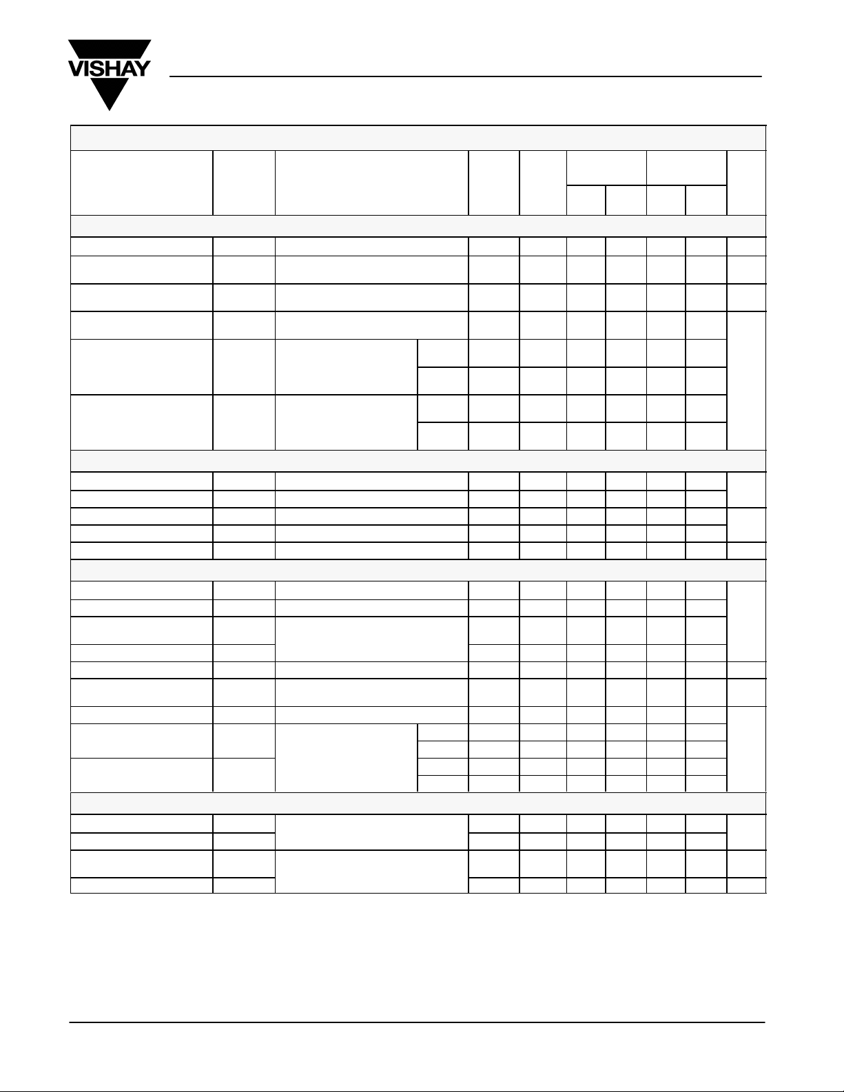
SPECIFICATIONS
Parameter Symbol
a
Test Conditions
Unless Otherwise Specified
V+ = 15 V, V- = -15 V
= 0.8 V, VAH = 2.4 V
V
AL
f
TempbTypcMindMaxdMindMaxdUnit
A Suffix
-55 to 125_C
D Suffix
-40 to 85_C
Analog Switch
Analog Signal Range
Drain-Source On-Resistance r
r
Matching Between
DS(on)
g
Channels
Source Off
Leakage Current
Drain Off Leakage Current I
Drain On Leakage Current I
e
V
ANALOG
DS(on)
r
DS(on)
I
S(off)
D(off)
D(on)
Full -15 15 -15 15 V
VD = "10 V, IS = -10 mA
VD = "10 V Room 15 15 %
VS = "10 V, V
VD = "10 V
V
= #10 V
S
= 0 V
V
EN
VS = VD = "10 V
Sequence Each
Switch On
= #10 V
D
= 0 V
V
EN
DG408
DG409
DG408
DG409
Room
Full
Room
Full
Room
Full
Room
Full
Room
Full
Room
Full
40 100
-1001100-1-20
-1001100-1-20
-0.5
-50
-1
-1
-50
-1
-1
-50
125
0.550-0.5-50.5
1
50-1-10
1
50-1-10
100
125
20
10
20
10
5
1
1
nA
1
1
Digital Control
Logic High Input Voltage V
Logic Low Input Voltage V
Logic High Input Current I
Logic Low Input Current I
Logic Input Capacitance C
INH
INL
AH
AL
VA = 2.4 V, 15 V Full -10 10 -10 10
VEN = 0 V, 2.4 V, VA = 0 V Full -10 10 -10 10
in
f = 1 MHz Room 8 pF
Full 2.4 2.4
Full 0.8 0.8
A
Dynamic Characteristics
Transition Time t
Break-Before-Make Interval t
Enable Turn-On Time t
Enable Turn-Off Time t
Charge Injection Q CL = 10 nF, VS = 0 V Room 20 pC
Off Isolation
Source Off Capacitance C
Drain Off Capacitance C
Drain On Capacitance C
h
TRANS
OPEN
ON(EN)
OFF(EN)
OIRR
S(off)
D(off)
D(on)
VEN = 0 V, VD = 0 V
VEN = 0 V, VD = 0 V
See Figure 2 Full 160 250 250
See Figure 4 Room 10 10
Room
See Figure 3
See Figure 3
VEN = 0 V, RL = 1 k
f = 100 kHz
VEN = 0 V, VS = 0 V, f = 1 MHz Room 3
DG408 Room 26
DG409 Room 14
f = 1 MHz
DG408 Room 37
DG409 Room 25
Full
Room 105 150 150
Room -75 dB
115 150
225
150
ns
pF
Power Supplies
Positive Supply Current I+ Full 10 75 75
Negative Supply Current I-
Positive Supply Current I+
Negative Supply Current I-
VEN = VA = 0 V or 5 V
VEN = 2.4 V, VA = 0 V
VEN = 2.4 V, VA = 0 V
Full 1 -75 -75
Room
Full
Full -500 -500
0.2 0.5
2
0.5
A
mA
2
A
V
Document Number: 70062
S-03081—Rev. F, 27-Jan-03
www.vishay.com
3
Page 4
DG408/409
Vishay Siliconix
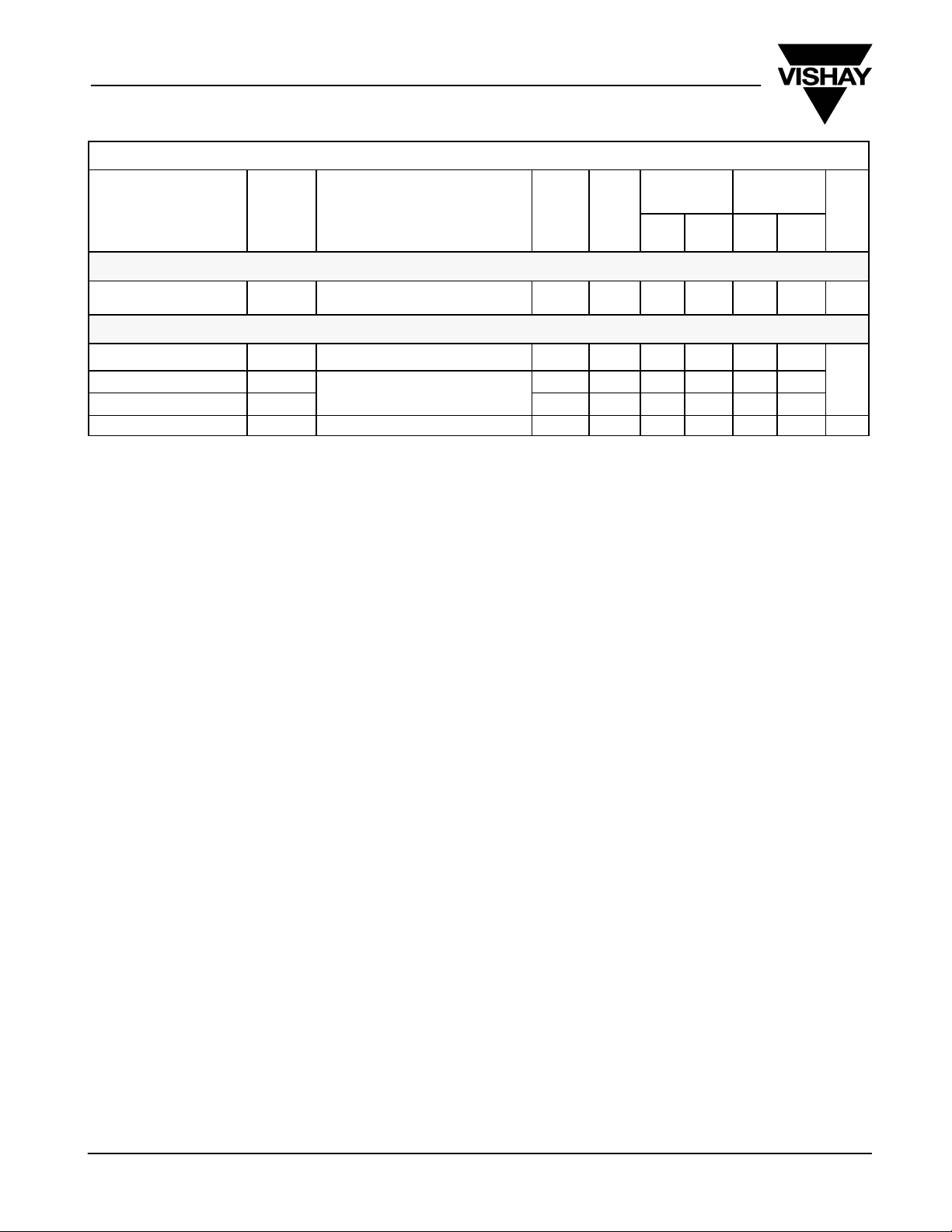
SPECIFICATIONSa FOR SINGLE SUPPLY
Parameter Symbol
Test Conditions
Unless Otherwise Specified
V+ = 12 V, V- = 0 V
= 0.8 V, VAH = 2.4 V
V
AL
f
TempbTypcMindMaxdMindMaxdUnit
A Suffix
-55 to 125_C
Analog Switch
Drain-Source
On-Resistance
e, f
r
DS(on)
VD = 3 V, 10 V, IS = - 1 mA Room 90
Dynamic Characteristics
e
e
Max - r
e
t
TRANS
t
ON(EN)
t
OFF(EN)
Q CL = 1 nF, VS= 6 V, RS = 0 Room 5 pC
Min.
DS(on)
VS1 = 8 V, VS8 = 0 V, VIN = 2.4 V Room 180
V
V
INH
INH
= 2.4 V, V
= 2.4 V, V
= 5 V
V
S1
INL
INL
= 0 V
= 0 V
Room 180
Room 120
Switching Time of Multiplexer
Enable Turn On Time
Enable Turn Off Time
Charge Injection
Notes
a. Refer to PROCESS OPTION FLOWCHART.
b. Room = 25_C, Full = as determined by the operating temperature suffix.
c. Typical values are for DESIGN AID ONLY, not guaranteed nor subject to production testing.
d. The algebraic convention whereby the most negative value is a minimum and the most positive a maximum, is used in this data sheet.
e. Guaranteed by design, not subject to production test.
f. V
IN
g. r
DS(on)
h. Worst case isolation occurs on Channel 4 do to proximity to the drain pin.
e
= input voltage to perform proper function.
= r
DS(on)
D Suffix
-40 to 85_C
ns
www.vishay.com
4
Document Number: 70062
S-03081—Rev. F, 27-Jan-03
Page 5

TYPICAL CHARACTERISTICS (25_C UNLESS NOTED)
DG408/409
Vishay Siliconix
Source/Drain Capacitance vs. Analog Voltage
80
V+ = 15 V
V- = -15 V
(pF)C
S, D
(pA)
D
I
100
-20
-60
-100
60
40
20
0
-10 -5 5 10
V+ = 15 V
V- = -15 V
= -VD for I
V
60
S
VD = V
20
V
ANALOG
S(open)
DG409 I
DG408 I
C
D(on)
C
D(off)
C
S(off)
015-15
- Analog Voltage (V)
D(off)
for I
D(on)
D(off)
DG409 I
, I
D(on)
D(off)
D(on)
Drain Leakage Current vs. Source/Drain Voltage
(Single 12-V Supply)
D(off)
D(on)
DG409 I
D(on)
D(off)
DG408 I
VD - Drain Voltage (V)
DG408 I
D(on)
(pA)
D
I
-20
-40
-60
60
40
20
0
VS = 0 V for I
VS = VD for I
DG409 I
Source Leakage Current vs. Source VoltageDrain Leakage Current vs. Source/DrainVoltage
20
15
V+ = 15 V
V- = -15 V
V+ = 12 V
V- = 0 V
(pA)
S(off)
I
10
5
0
-5
D(off)
12010624 8
-140
-10 -5 5 10 0 15-15
VD or VS — Drain or Source Voltage (V) VS - Source Voltage (V)
Input Switching Threshold vs. Supply Voltage
2.0
1.5
(V)
1.0
TH
V
0.5
0.0
Document Number: 70062
S-03081—Rev. F, 27-Jan-03
015-15
12 2048 16
+V
SUPPLY
(V)
-100 mA
I-
-10
-10 -5 5 10
Negative Supply Current vs. Switching Frequency
V
= "15 V
-10 mA
-1 mA
-100 A
-10 A
-1 A
-0.1 A
SUPPLY
V
= 2.4 V
EN
10 k 10 M100 1 k 100 k 1 M
Switching Frequency (Hz)
VEN = 0 V or 5 V
www.vishay.com
5
Page 6

DG408/409
Vishay Siliconix
TYPICAL CHARACTERISTICS (25_C UNLESS NOTED)
Positive Supply Current vs. Switching Frequency I
100 mA
10 mA
I+
100 A
I+ ( A)
1 mA
10 A
20
15
10
V
= "15 V
SUPPLY
V
= 2.4 V
EN
VEN = 0 V or 5 V
10 k 10 M100 1 k 100 k 1 M
Switching Frequency (Hz)
V+ = 15 V
V- = -15 V
= 0 V
V
IN
= 0 V
V
EN
5
0
-35 -15 25 65 105
Temperature (_C)
125-55 85455
100 mA
I+, I-
Q (pC)
10 mA
1 mA
100 nA
10 nA
1 nA
100 pA
10 pA
90
80
70
60
50
40
30
20
10
-10
vs. Temperature
SUPPLY
I+
-(I-)
-35 -15 25 65 105
Temperature (_C)
V
SUPPLY
= 0 V
V
A
V
EN
Charge Injection vs. Analog VoltagePositive Supply Current vs. Temperature (DG408)
CL = 10,000 pF
= 5 Vp-p
V
IN
V+ = 15 V
V- = -15 V
0
-10 -5 5 10
V
S
015-15
- Source Voltage (V)
= 0 V
= "15 V
V+ = 12 V
V- = 0 V
125-55 85455
120
100
80
()
60
DS(on)
r
40
20
0
-20 -12 -8 -4 0 4 8 12 16 20-16
www.vishay.com
6
r
vs. VD and Supply r
DS(on)
"5 V
"8 V
"10 V
"12 V
"20 V
VD - Drain Voltage (V) VD - Drain Voltage (V)
"15 V
160
140
120
100
()
DS(on)
r
80
60
40
20
0
vs. VD and Supply (Single Supply)
DS(on)
V+ = 7.5 V
10 V
V- = 0 V
4 8 12 16 20
12 V
15 V
Document Number: 70062
S-03081—Rev. F, 27-Jan-03
20 V
22 V
220
Page 7

TYPICAL CHARACTERISTICS (25_C UNLESS NOTED)
r
vs. VS and Temperature r
DS(on)
V+ = 15 V
V- = -15 V
125_C
85_C
25_C
0_C
-40_C
-10 -5 5 10
VS - Source Voltage (V) VS - Source Voltage (V)
-55_C
015-15
Off Isolation and Crosstalk vs. Frequency Insertion Loss vs. Frequency
V+ = 15 V
V- = -15 V
R
= 1 k
L
Off-Isolation
Crosstalk
()
DS(on)
r
-150
-130
-110
-90
(dB)
-70
-50
80
70
60
50
40
30
20
10
0
130
110
90
()
70
DS(on)
r
50
30
10
1
0
-1
-2
-3
LOSS (dB)
-4
-5
DG408/409
Vishay Siliconix
vs. VS and Temperature (Single Supply)
DS(on)
125_C
85_C
25_C
0_C
-40_C
-55_C
V+ = 12 V
V- = 0 V
2610
RL = 1 k
V+ = 15 V
V- = -15 V
Ref. 1 Vrms
RL = 50
12840
-30
100 1 k 100 k 1 M
200
175
150
t (ns)
125
100
75
"10 "12 "14 "16 "18 "20 "22
Document Number: 70062
S-03081—Rev. F, 27-Jan-03
-6
10 k 10 M
f - Frequency (Hz) f - Frequency (Hz)
100 M
10 100 1 k 10 k 100 k 1 M 100 M
Switching Time vs. Single SupplySwitching Time vs. Bipolar Supply
275
t
t
ON(EN)
TRANS
t
OFF(EN)
V
(V) V
SUPPLY
t (ns)
250
225
200
175
150
125
100
91214131110
t
ON(EN)
SUPPLY
(V)
t
TRANS
10 M
t
OFF(EN)
www.vishay.com
158
7
Page 8
DG408/409
Vishay Siliconix
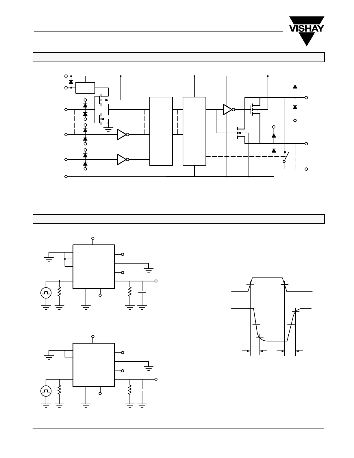
SCHEMATIC DIAGRAM (TYPICAL CHANNEL)
V+
GND
A
0
A
X
EN
V-
TEST CIRCUITS
A
2
A
1
A
0
EN
50
V
REF
DG408
V+
V+
+15 V
S2 - S
V-GND
-15 V
D
V+
Level
Shift
Decode/
Drive
V-
S
1
S
n
FIGURE 1.
1
7
8
D
300
"10 V
#10 V
35 pF
tr <20 ns
<20 ns
t
V
O
Logic
Input
3 V
50%
f
0 V
V
Switch
Output
V
O
S1
0 V
90%
S
S
www.vishay.com
8
50
A
A
EN
1
0
+15 V
V+
S1a - S4a, D
DG409
V-GND
-15 V
V
S8
t
1
a
b
300
"10 V
#10 V
35 pF
V
O
S
S
4b
D
TRANS
1
ON
90%
S
t
ONS
8
TRANS
FIGURE 2. Transition Time
Document Number: 70062
S-03081—Rev. F, 27-Jan-03
Page 9

TEST CIRCUITS
DG408/409
Vishay Siliconix
+15 V
50
50
V+
EN
A
0
DG408
A
1
A
2
GND V-
+15 V
V+
EN
A
0
A
1
S1a - S4a, D
DG409
GND V-
S2 - S
-15 V
S2b - S
-15 V
S
D
S
1b
a
4b
D
b
1
8
1 k
1 k
- 5 V
- 5 V
35 pF
35 pF
V
O
Logic
Input
3 V
50%
tr <20 ns
<20 ns
t
f
0 V
t
ON(EN)
0 V
Switch
Output
V
O
V
O
V
O
90%
t
OFF(EN)
10%
+2.4 V
EN
A
A
A
50
Document Number: 70062
S-03081—Rev. F, 27-Jan-03
+15 V
V+
All S and D
0
DG408
1
DG409
2
GND V-
Db, D
-15 V
FIGURE 3. Enable Switching Time
+5 V
a
V
O
300
35 pF
FIGURE 4. Break-Before-Make Interval
Logic
Input
Switch
Output
V
O
3 V
0 V
0 V
tr <20 ns
<20 ns
t
f
50%
V
S
80%
t
OPEN
www.vishay.com
9
Page 10

DG408/409
Vishay Siliconix
TEST CIRCUITS
R
g
Channel
Select
V
IN
S
V
S
Rg = 50
X
S
8
A
0
A
1
A
2
S
X
EN
V+
A
0
A
1
A
2
GND V-
+15 V
V+
EN
GND V-
+15 V
-15 V
C
L
10 nF
V
O
D
FIGURE 5. Charge Injection
D
R
L
1 k
V
O
Switch
Output
Rg = 50
Logic
Input
3 V
OFF ON
0 V
VO is the measured voltage due to charge transfer
error Q, when the channel turns off.
Q = C
x V
L
O
+15 V
V
IN
S
1
S
V
S
X
S
8
A
0
A
1
A
2
V+
GND V-
EN
D
OFF
V
R
L
1 k
O
V
O
V
S
Rg = 50
-15 V
Off Isolation = 20 log
V
OUT
V
IN
-15 V
Crosstalk = 20 log
FIGURE 6. Off Isolation FIGURE 7. Crosstalk
+15 V
S
1
A
0
A
1
A
2
V+
GND V-
EN
D
-15 V
Insertion Loss = 20 log
FIGURE 8. Insertion Loss
R
L
1 k
Channel
V
O
Select
V
OUT
V
IN
+15 V
A
A
A
2
1
0
GND
V+
EN
S
1
S
8
D
V-
-15 V
FIGURE 9. Source Drain Capacitance
V
OUT
V
IN
Meter
HP4192A
Impedance
Analyzer
or Equivalent
f = 1 MHz
www.vishay.com
10
Document Number: 70062
S-03081—Rev. F, 27-Jan-03
Page 11

APPLICATION HINTS
Overvoltage Protection
DG408/409
Vishay Siliconix
A very convenient form of overvoltage protection consists of
adding two small signal diodes (1N4148, 1N914 type) in series
with the supply pins (see Figure 10). This arrangement
effectively blocks the flow of reverse currents. It also floats the
supply pin above or below the normal V+ or V- value. In this
case the overvoltage signal actually becomes the power
V+
S
X
V
g
V-
FIGURE 10. Overvoltage Protection Using Blocking Diodes
8-Channel Sequential Multiplexer/Demultiplexer
+15 V -15 V
supply of the IC. From the point of view of the chip, nothing has
changed, as long as the difference V
- (V-) doesn’t exceed
S
+44 V. The addition of these diodes will reduce the analog
signal range to 1 V below V+ and 1 V above V-, but it
preserves the low channel resistance and low leakage
characteristics.
1N4148
D
DG408
1N4148
Differential 4-Channel Sequential Multiplexer/Demultiplexer
+15 V -15 V
Analog
Inputs
(Outputs)
+15 V
Clock
In
NC
Enable In
(MUX On-Off Control)
Document Number: 70062
S-03081—Rev. F, 27-Jan-03
DM7493
B
IN
A
IN
r01r
+15 V
02
Q
Q
Q
Q
GND
B
C
D
A
GND
V+ V-
S
1
S
2
S
3
S
4
DG408
S
5
S
6
S
7
S
8
A0A1A
NC
2
EN
GNDV+ V-
S
1a
S
NC
S
S
S
S
S
S
2a
3a
4a
1b
2b
3b
4b
A
DG409
0A1
J
CLK
K
EN
D
a
Differential
Analog
Outputs
(Inputs)
D
b
Q
Q
NC
6
Analog
Output
(Input)
D
Clock
In
Reset Enable
Differential
Analog
Inputs
(Outputs)
+15 V
J
1/2 MM74C73 1/2 MM74C73
CLK
K
CLEAR CLEAR
Q
Q
GND
FIGURE 11.
www.vishay.com
11
 Loading...