

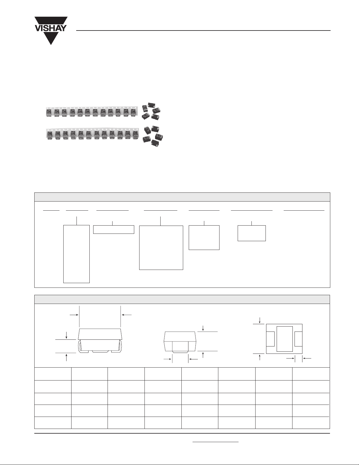
Solid Tantalum Chip Capacitors
TANTAMOUNT® Military, Surface Mount
MIL-PRF-55365/8 Qualified
FEATURES
• Molded case available in four case codes.
• Compatible with "High Volume" automatic pick and place
equipment.
• Weibull Failure Rates B and C.
• Termination: (H) Solder plate.
• Surge Current Option A
PERFORMANCE / ELECTRICAL CHARACTERISTICS
Operating Temperature: - 55°C to + 85°C. (To + 125°C with
voltage derating.)
Capacitance Range: 0.10µF to 100µF.
Capacitance Tolerance: ± 20%, ± 10% standard, ± 5%
available
Voltage Rating: 4 WVDC to 50 WVDC.
CWR11
Vishay Sprague
ORDERING INFORMATION
CWR11
TYPE
D
VOLTAGE
C = 4 V
D = 6 V
F = 10 V
H = 15 V
J = 20 V
K = 25 V
M = 35 V
N = 50 V
H
TERMINATION
FINISH
H = Solder Plate.
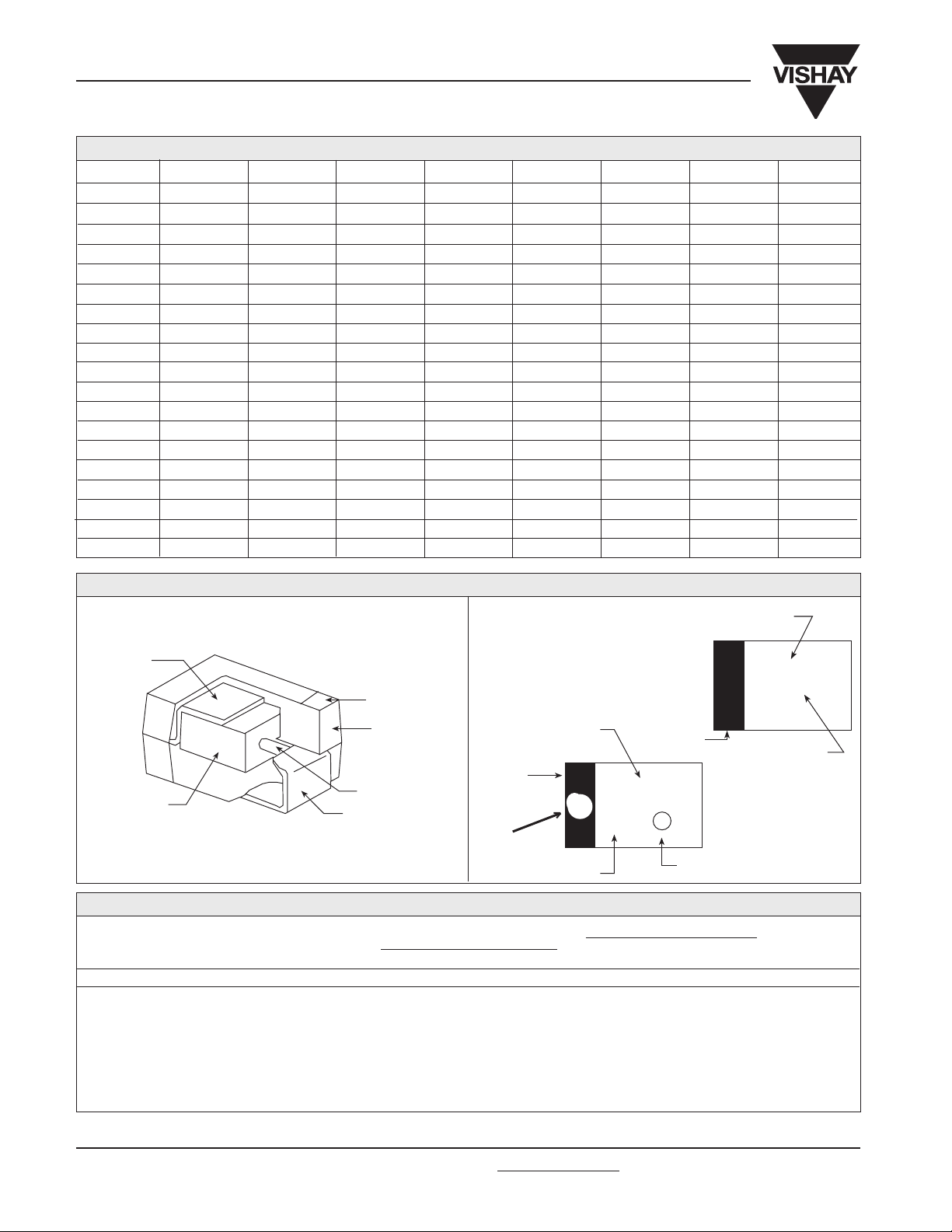
DIMENSIONS In inches [millimeters]
L
TH Min.
155
CAPACITANCE
This is expressed
in picofarads. The
first two digits are
the significant
figures. The third
is the number of
zeros to follow.
CAPACITANCE
TOLERANCE
M= ± 20%
K=± 10%
J=± 5%
TW
K
WEIBULL FAILURE
RATE 1%/1000 HOURS
H
B
SURGE CURRENT
B = 0.1
C = 0.01
W
A
OPTION
P
CASE
CODE
A
B
C
D
Document Number 40011
Revision 31-Jan-05
EIA
SIZE
3216
3528
6032
7343
L
0.126 ± 0.008
[3.2 ± 0.20]
0.138 ± 0.008
[3.5 ± 0.20]
0.236 ± 0.012
[6.0 ± 0.30]
0.287 ± 0.012
[7.3 ± 0.30]
For technical questions, contact tantalum@vishay.com
W
0.063 ± 0.008
[1.6 ± 0.20]
0.110 ± 0.008
[2.8 ± 0.20]
0.126 ± 0.012
[3.2 ± 0.30]
0.170 ± 0.012
[4.3 ± 0.30]
H
0.063 ± 0.008
[1.6 ± 0.20]
0.075 ± 0.008
[1.9 ± 0.20]
0.098 ± 0.012
[2.5 ± 0.30]
0.110 ± 0.012
[2.8 ± 0.30]
P
0.031 ± 0.012
[0.80 ± 0.30]
0.031 ± 0.012
[0.80 ± 0.30]
0.051 ± 0.012
[0.80 ± 0.30]
0.051 ± 0.012
[1.3 ± 0.30]
TW
0.047 ± 0.004
[1.2 ± 0.10]
0.087 ± 0.004
[2.2 ± 0.10]
0.087 ± 0.004
[2.2 ± 0.10]
0.095 ± 0.004
[2.4 ± 0.10]
TH (Min.)
0.028
[0.70]
0.028
[0.70]
0.039
[1.0]
0.039
[1.0]
www.vishay.com
47
CWR11
Vishay Sprague
RATINGS AND CASE CODES
µF
0.10
0.15
0.22
0.33
0.47
0.68
1.0
1.5
2.2
3.3
4.7
6.8
10
15
22
33
47
68
100
4 V
A
A
B
B
B
C
D
D
6 V
A
A
A
B
B
B
C
C
D
D
10 V
A
A
A
B
B
B
C
D
D
15 V
A
A
A
B
B
B
C
D
D
20 V
A
A
A
B
B
B
C
C
D
D
25 V
A
A
B
B
B
C
C
C
D
D
D
35 V
A
A
A
A
B
B
B
C
C
C
D
D
50 V
A
B
B
B
C
C
C
D
D
D
D
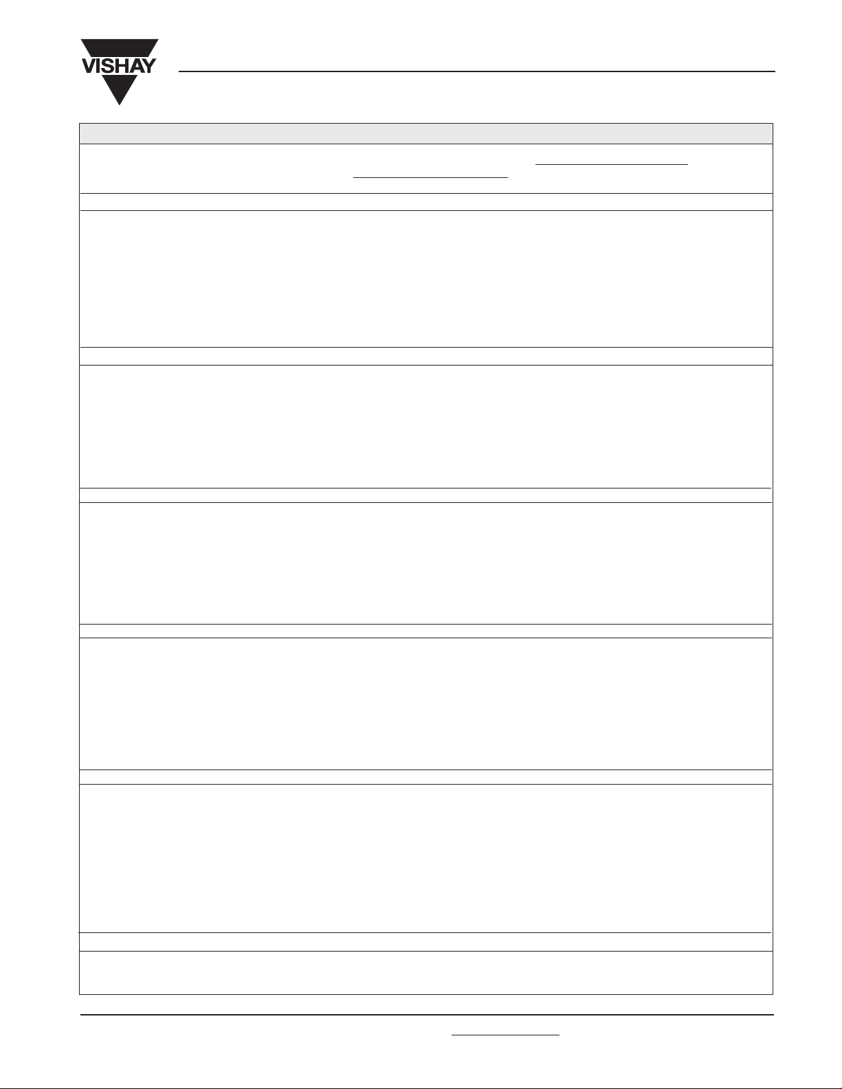
CONSTRUCTION MARKING
Cathode
Termination ( - )
Tantalum
Capacitor
Element
CONSTRUCTION MARKING
Polarity Stripe ( + )
Epoxy Case
Anode Weld
Positive
Termination
Polarity
Band
B, C, and D
Cases
"JAN" Brand
Capacitance
J
Voltage
Polarity Band
105
35
Capacitance Code, pf
2
Vishay Sprague Logo
STANDARD RATINGS
CAPACITANCE
(µF)
CASE
CODE
PART NUMBER
Max. DC Leakage (µA) @
+ 85°C
4 WVDC @ + 85°C, SURGE = 5.2 V . . . 2.7 WVDC @ + 125°C, SURGE = 3.4 V
2.2 A CWR11CH225#* 0.5 5 6 6 9 9 8
4.7 A CWR11CH475#* 0.5 5 6 6 9 9 8
6.8 B CWR11CH685#* 0.5 5 6 6 9 9 5.5
10 B CWR11CH106#* 0.5 5 6 6 9 9 4
15 B CWR11CH156#* 0.6 6 7.2 6 6 9 3.5
33 C CWR11CH336#* 1.3 13.0 15.6 6 9 9 2.2
68 D CWR11CH686#* 2.7 27 32.4 6 9 9 1.1
100 D CWR11CH107#* 4 40 48 8 12 12 0.9
# = Tolerance: J = ± 5%, K = ± 10%, M = ± 20%. * = Weibull Failure Rate (%/1,000 hours): B = 0.1, C = 0.01, D = 0.001
Max. DF 120 Hz (%) @
+ 25°C+ 125°C+ 25°C
+ 85°C
+ 125°C
- 55°C
105J
"JAN" Brand
Max. ESR
@ + 25°C
100kHz
(Ohms)
www.vishay.com
48
For technical questions, contact tantalum@vishay.com
Document Number 40011
Revision 31-Jan-05
Vishay Sprague
STANDARD RATINGS
Max. DF 120 Hz (%) @
CAPACITANCE
(µF)
1.5 A CWR11DH155#* 0.5 5 6 6 9 9 8
2.2 A CWR11DH225#* 0.5 5 6 6 6 9 8
3.3 A CWR11DH335#* 0.5 5 6 6 9 9 8
4.7 B CWR11DH475#* 0.5 5 6 6 9 9 5.5
6.8 B CWR11DH685#* 0.5 5 6 6 6 9 4.5
10 B CWR11DH106#* 0.6 6 7.2 6 9 9 3.5
15 C CWR11DH156#* 0.9 9.0 10.8 6 6 9 3.0
22 C CWR11DH226#* 1.4 14.0 16.8 6 9 9 2.2
47 D CWR11DH476#* 2.8 28 33.6 6 6 9 1.1
68 D CWR11DH686#* 4.3 43 51.6* 6 9 9 0.9
1 A CWR11FH105#* 0.5 5 6 4 6 6 10
1.5 A CWR11FH155#* 0.5 5 6 6 6 9 8
2.2 A CWR11FH225#* 0.5 5 6 6 9 9 8
3.3 B CWR11FH335#* 0.5 5 6 6 9 9 5.5
4.7 B CWR11FH475#* 0.5 5 6 6 9 9 4.5
6.8 B CWR11FH685#* 0.7 7 8.4 6 9 9 3.5
15 C CWR11FH156#* 1.5 15 18.0 6 6 9 2.5
33 D CWR11FH336#* 3.3 33 39.6 6 6 9 1.1
47 D CWR11FH476#* 4.7 47 56.4 6 9 9 0.9
0.68 A CWR11HH684#* 0.5 5 6 4 6 6 12
1 A CWR11HH105#* 0.5 5 6 4 6 6 10
1.5 A CWR11HH155#* 0.5 5 6 6 9 9 8
2.2 B CWR11HH225#* 0.5 5 6 6 9 9 5.5
3.3 B CWR11HH335#* 0.5 5 6 6 8 9 5
4.7 B CWR11HH475#* 0.7 7 8.4 6 9 9 4
10 C CWR11HH106#* 1.6 16 19.2 6 8 9 2.5
22 D CWR11HH226#* 3.3 33 39.6 6 8 9 1.1
33 D CWR11HH336#* 5.3 53 63.6 6 9 9 0.9
0.47 A CWR11JH474#* 0.5 5 6 4 6 6 14
0.68 A CWR11JH684#* 0.5 5 6 4 6 6 12
1 A CWR11JH105#* 0.5 5 6 4 6 6 10
1.5 B CWR11JH155#* 0.5 5 6 6 9 9 6
2.2 B CWR11JH225#* 0.5 5 6 6 8 9 5
3.3 B CWR11JH335#* 0.7 7 8.4 6 9 9 4
4.7 C CWR11JH475#* 1.0 10 12 6 8 9 3.0
6.8 C CWR11JH685#* 1.4 14 16.8 6 9 9 2.4
15 D CWR11JH156#* 3 30 36 6 8 9 1.1
22 D CWR11JH226#* 4.4 44 52.8 6 9 9 0.9
0.33 A CWR11KH334#* 0.5 5.0* 6 4 6 6 15
0.47 A CWR11KH474#* 0.5 5.0* 6 4 6 6 14
0.68 B CWR11KH684#* 0.5 5.0* 6 4 6 6 7.5
1 B CWR11KH105#* 0.5 5.0* 6 4 6 6 6.5
1.5 B CWR11KH155#* 0.5 5.0* 6 6 8 9 6.5
2.2 C CWR11KH225#* 0.6 6.0 7.2 6 9 9 3.5
3.3 C CWR11KH335#* 0.9 9.0 10.8 6 8 9 2.5
4.7 C CWR11KH475#* 1.2 12 14.4 6 9 9 2.5
6.8 D CWR11KH685#* 1.7 17.0* 20.4 6 9 9 1.4
10 D CWR11KH106#* 2.5 25.0* 30 6 8 9 1.2
15 D CWR11KH156#* 3.8 38.0* 45.6 6 9 9 1
0.1 A CWR11MH104#* 0.5 5 6 4 6 6 24
0.15 A CWR11MH154#* 0.5 5 6 4 6 6 21
0.22 A CWR11MH224#* 0.5 5 6 4 6 6 18
# = Tolerance: J = ± 5%, K = ± 10%, M = ± 20% *= Weibull Failure Rate (%/1,000 hours): B = 0.1, C = 0.01, D = 0.001
CASE
CODE
PART NUMBER
6 WVDC @ + 85°C, SURGE = 8 V . . . 4 WVDC @ + 125°C, SURGE = 5 V
10 WVDC @ + 85°C, SURGE = 13 V . . . 7 WVDC @ + 125°C, SURGE = 8 V
15 WVDC @ + 85°C, SURGE = 20 V . . . 10 WVDC @ + 125°C, SURGE = 12 V
20 WVDC @ + 85°C, SURGE = 26 V . . . 13 WVDC @ + 125°C, SURGE = 16 V
25 WVDC @ + 85°C, SURGE = 32 V . . . 17 WVDC @ + 125°C, SURGE = 20 V
35 WVDC @ + 85
°C, SURGE = 46 V . . . 23 WVDC @ + 125°C, SURGE = 28 V
Max. DC Leakage (µA) @
+ 25°C
+ 125°C+ 85°C
+ 25
°C
+ 85°C
+ 125°C
- 55
CWR11
Max. ESR
@ + 25°C
°C
100kHz
(Ohms)
Document Number 40011
Revision 31-Jan-05
For technical questions, contact tantalum@vishay.com
www.vishay.com
49
CWR11
Vishay Sprague
STANDARD RATINGS
CAPACITANCE
µF)
(
0.33 A CWR11MH334#* 0.5 5 6 4 6 6 15
0.47 B CWR11MH474#* 0.5 5 6 4* 6 6 10
0.68 B CWR11MH684#* 0.5 5 6 4 6 6 8
1 B CWR11MH105#* 0.5 5 6 4 6 6 6.5
1.5 C CWR11MH155#* 0.5 5 6 6 8 9 4.5
2.2 C CWR11MH225#* 0.8 8 9.6 6 8 9 3.5
3.3 C CWR11MH335#* 1.2 12 14.4 6 8 9 2.5
4.7 D CWR11MH475#* 1.7 17 20.4 6 8 9 1.5
6.8 D CWR11MH685#* 2.4 24 28.8 6 9 9 1.3
0.1 A CWR11NH104#* 0.5 5 6 4 6 6 22
0.15 B CWR11NH154#* 0.5 5 6 4 6 6 17
0.22 B CWR11NH224#* 0.5 5 6 4 6 6 14
0.33 B CWR11NH334#* 0.5 5 6 4 6 6 12
0.47 C CWR11NH474#* 0.5 5 6 4 6 6 8
0.68 C CWR11NH684#* 0.5 5 6 4 6 6 7
1 C CWR11NH105#* 0.5 5 6 4 6 6 6
1.5 D CWR11NH155#* 0.8 8 9.6 6 8 9 4
2.2 D CWR11NH225#* 1.1 11 13.2 6 8 9 2.5
3.3 D CWR11NH335#* 1.7 17 20.4 6 9 9 2
4.7 D CWR11NH475#* 2.4 24 28.8 6 9 9 1.5
# = Tolerance: J = ± 5%, K = ± 10%, M = ± 20%.
* = Weibull Failure Rate (%/1,000 hours): B = 0.1, C = 0.01, D = 0.001
CASE
CODE - 55°C
35 WVDC @ + 85°C, SURGE = 46 V . . . 23 WVDC @ + 125°C, SURGE = 28 V
50 WVDC @ + 85°C, SURGE = 65 V . . . 33 WVDC @ + 125°C, SURGE = 40 V
Max. DC Leakage (µA) @
+ 125°C+ 85°CPART NUMBER* + 25°C
Max. DF 120 Hz (%) @
+ 85°C
+ 25°C
+ 125°C
Max. ESR
@ + 25
°C
100kHz
(Ohms)
PERFORMANCE CHARACTERISTICS
1. Operating Temperature: Capacitors are designed to
operate over the temperature range of - 55°C to + 85°C.
1.1 Capacitors may be operated to + 125°C with voltage
derating to two-thirds the + 85°C rating.
+ 85°C Rating + 125°C Rating
Working
Voltage
(V)
4
6.3
10
16
20
25
35
Surge
Voltage
(V)
5.2
8
13
20
26
32
46
2. DC Working Voltage: The DC working voltage is the
maximum operating voltage for continuous duty at the
rated temperature.
3. Surge Voltage: The surge DC rating is the maximum
voltage to which the capacitors may be subjected
under any conditions, including transients and peak
ripple at the highest line voltage.
3.1 Surge Voltage Test: Capacitors shall withstand the
surge voltage applied in series with a 33 ohm ± 5%
resistor at the rate of one-half minute on, one-half
minute off, at + 85°C, for 1000 successive test cycles.
3.2 Following the surge voltage test, the dissipation factor
Working
Voltage
(V)
2.7
4
7
10
13
17
23
Surge
Voltage
(V)
3.4
5
8
12
16
20
28
and the leakage current shall meet the initial requirements; the capacitance shall not have changed
more than ± 10%.
4. Capacitance Tolerance: The capacitance of all
capacitors shall be within the specified tolerance
limits of the normal rating.
4.1 Capacitance measurements shall be made by means
of polarized capacitance bridge. The polarizing
voltage shall be of such magnitude that there shall be
no reversal of polarity due to the AC component.
The maximum voltage applied to capacitors during
measurement shall be 2 volts rms at 120 Hz at
+ 25°C. If the AC voltage applied is less than onehalf volt rms, no DC bias is required. Accuracy of the
bridge shall be within ± 2%.
5. Capacitance Change With Temperature: The
capacitance change with temperature shall not
exceed the following percentage of the capacitance
measured at + 25°C:
- 55°C
- 10%
+ 85°C
+ 10%
+ 125°C
+ 12%
6. Dissipation Factor: The dissipation factor,
determined from the expression 2πfRC, shall not
exceed values listed in the Standard Ratings Table.
6.1 Measurements shall be made by the bridge method
at, or referred to, a frequency of 120 Hz and a
temperature of + 25°C.
www.vishay.com
50
For technical questions, contact tantalum@vishay.com
Document Number 40011
Revision 31-Jan-05

CWR11
Vishay Sprague
PERFORMANCE CHARACTERISTICS (Continued)
7. Leakage Current: Capacitors shall be stabilized at
the rated temperature for 30 minutes. Rated voltage
shall be applied to capacitors for 5 minutes using a
steady source of power (such as a regulated power
supply) with a 1000 ohm resistor connected in series
with the capacitor under test to limit the charging
current. Leakage current shall then be measured.
Note that the leakage current varies with temperature and
applied voltage. See graph below for the appropriate
adjustment factor.
TYPICAL LEAKAGE CURRENT FACTOR RANGE
100
+ 125°C
+ 85°C
10
+ 55°C
+ 25°C
1.0
0°C
change shall not exceed ± 10%; the leakage
current shall not exceed 125% of the initial
requirement.
9. Vibration Tests: Capacitors shall be subjected to
vibration tests in accordance with the following
criteria.
9.1 Capacitors shall be secured for test by means of a
rigid mounting using suitable brackets.
9.2 Low Frequency Vibration: Vibration shall consist
of simple harmonic motion having an amplitude of
0.03" [0.76mm] and a maximum total excursion of
0.06" [1.52mm], in a direction perpendicular to the
major axis of he capacitors.
9.2.1 Vibration frequency shall be varied uniformly
between the approximate limits of 10 Hz to 55 Hz
during a period of approximately one minute,
continuously for 1.5 hours.
9.2.2 An oscilloscope or other comparable means shall
be used in determining electrical intermittency
during the final 30 minutes of the test. The AC
voltage applied shall not exceed 2 volts rms.
9.2.3 Electrical tests shall show no evidence of
intermittent contacts, open circuits or short circuits
during these tests.
0.1
Leakage Current Factor
- 55°C
0.01
0.001
0 10 20 30 40 50 60 70 80 90 100
Percent of Rated Voltage
7.1 At + 25°C, the leakage current shall not exceed the
value listed in the Standard Ratings Table.
7.2 At + 85
°C, the leakage current shall not exceed 10
times the value listed in the Standard Ratings Table.
7.3 At + 125
°C, the leakage current shall not exceed 12
times the value listed in the Standard Ratings Table.
8. Life Test: Capacitors shall withstand rated DC
voltage applied at + 85°C or two-thirds rated voltage
applied at + 125°C for 2000 hours.
9.2.4 Following the low frequency vibration test,
capacitors shall meet the original requirements for
capacitance, dissipation factor and leakage current.
9.3 High Frequency Vibration: Vibration shall
consist of a simple harmonic motion having an
amplitude of 0.06" [1.52] ± 10% maximum total
excursion or 20 g peak whichever is less.
9.3.1 Vibration frequency shall be varied logarithmically
from 50 Hz to 2000 Hz and return to 50 Hz during
a cycle period of 20 minutes.
9.3.2 The vibration shall be applied for 4 hours in each
of 2 directions, parallel and perpendicular to the
major axis of the capacitors.
9.3.3 Rated DC voltage shall be applied during the
vibration cycling.
9.3.4 An oscilloscope or other comparable means shall
be used in determining electrical intermittency
during the last cycle. The AC voltage applied shall
not exceed 2 volts rms.
9.3.5 Electrical tests shall show no evidence of
intermittent contacts, open circuits or short circuits
during these tests.
8.1 Following the life test, the dissipation factor shall
meet the initial requirement; the capacitance
Document Number 40011
Revision 31-Jan-05
For technical questions, contact tantalum@vishay.com
9.3.6 There shall be no mechanical damage to these
capacitors as a result of these tests.
www.vishay.com
51

CWR11
Vishay Sprague
PERFORMANCE CHARACTERISTICS (Continued)
9.3.7 Following the high frequency vibration test,
capacitors shall meet the original limits for
capacitance, dissipation factor and leakage
current.
10. Acceleration Test:
10.1 Capacitors shall be rigidly mounted by means of
suitable brackets.
10.2 Capacitors shall be subjected to a constant
acceleration of 100 g for a period of 10 seconds in
each of 2 mutually perpendicular planes.
10.2.1 The direction of motion shall be parallel to and
perpendicular to the longitudinal axis of the
capacitors.
10.3 Rated DC voltage shall be applied during
acceleration test.
10.3.1 An oscilloscope or other comparable means shall
be used in determining electrical intermittency
during test. The AC voltage applied shall not
exceed 2 volts rms.
10.4 Electrical tests shall show no evidence of
intermittent contacts, open circuits or short circuits
during these tests.
10.5 There shall be no mechancial damage to these
capacitors as a result of these tests.
10.6 Following the acceleration test, capacitors shall
meet the original limits for capacitance, dissipation
factor and leakage current.
11. Shock Test:
11.1 Capacitors shall be rigidly mounted by means of
suitable brackets. The test load shall be
distributed uniformly on the test platform to
minimize the effects of unbalanced loads.
11.1.1 Test equipment shall be adjusted to produce a
shock of 100 g peak with the duration of 6 mS and
sawtooth waveform at a velocity change of 9.7 ft./
sec.
11.2 Capacitors shall be subjected to 3 shocks applied
in each of 3 directions corresponding to the 3
mutually perpendicular axes of the capacitors.
11.3 Rated DC voltage shall be applied during test.
11.3.1 An oscilloscope or other comparable means shall
be used in determining electrical intermittency
during tests. The replacement voltage applied
shall not exceed 2 volts rms.
11.4 Electrical tests shall show no evidence of
intermittent contacts, open circuits or short circuits
during these tests.
11.5 There shall be no mechanical damage to these
capacitors as a result of these tests.
11.6 Following the shock test, capacitors shall meet the
original limits for capacitance, dissipation factor
and leakage current.
12. Moisture Resistance:
12.1 Capacitors shall be subjected to temperature
cycling at 90% to 95% relative humidity, from
+ 25°C to + 65°C to + 25°C (+ 10°C, - 2°C) over a
period of 8 hours per cycle for 1000 hours.
12.2 Following the moisture resistance test, the leakage
current and dissipation factor shall meet the initial
requirements, and the change in capacitance shall
not exceed ± 10%.
13. Thermal Shock:
13.1 Capacitors shall be conditioned prior to
temperature cycling for 15 minutes at + 25°C, at
less than 50% relative humidity and a barometric
pressure at 28 to 31 inches.
13.2 Capacitors shall be subjected to thermal shock in a
cycle of exposure to ambient air at - 65°C (+ 0°C,
- 5°C) for 30 minutes, then + 25°C (+10°C, - 5°C)
for 5 minutes, then + 125°C (+ 3°C, - 0°C) for 30
minutes, then + 25°C (+ 10°C, - 5°C) for 5 minutes
for 5 cycles.
13.3 Capacitors shall show no evidence of harmful or
extensive corrosion, obliteration of marking or
other visible damage.
13.4 Following the thermal shock test, capacitors shall
meet the original requirements for leakage current
and dissipation factor, capacitance change shall
not exceed ± 5% of the original measured value.
14. Soldering Compatibility:
14.1 Resistance to Solder Heat: Capacitors will
withstand exposure to + 260ºC + 5ºC for 10
seconds.
14.1.1 Following the resistance to soldering heat test,
capacitance, dissipation factor and DC leakage
current shall meet the initial requirement.
14.2 Solderability: Capacitors will meet the
solderability requirements of ANSI / J-STD-002,
Test B (MIL-STD-202, method 208 and Test S).
14.3 Solderability:
solderability requirements of (MIL-STD-202
method 208), ANSI/J-STD-002, Test B.
Capacitors will meet the
www.vishay.com
52
For technical questions, contact tantalum@vishay.com
Document Number 40011
Revision 31-Jan-05

CWR11
Vishay Sprague
GUIDE TO APPLICATION
1. A-C Ripple Current: The maximum allowable ripple
current shall be determined from the formula:
P
=
I
rms
where,
P = Power Dissipation in Watts @ + 25°C as given
in the table in Paragraph Number 5 (Power
Dissipation).
= The capacitor Equivalent Series Resistance
R
ESR
at the specified frequency.
2. A-C Ripple Voltage: The maximum allowable ripple
voltage shall be determined from the formula:
V
rms
or, from the formula:
V
= I
rms
P = Power Dissipation in Watts @ + 25°C as
given in the table in Paragraph Number 5
(Power Dissipation).
= The capacitor Equivalent Series Resistance
R
ESR
at the specified frequency.
Z = The capacitor impedance at the specified
frequency.
2.1 The sum of the peak AC voltage plus the DC
voltage shall not exceed the DC voltage rating of the
capacitor.
2.2 The sum of the negative peak AC voltage plus the
applied DC voltage shall not allow a voltage reversal
exceeding 10% of the DC working voltage at + 25°C.
3. Reverse Voltage: These capacitors are capable of
withstanding peak voltages in the reverse direction
equal to 10% of the DC rating at + 25°C, 5% of the
DC rating at + 85°C and 1% of the DC rating at
+ 125°C.
4. Temperature Derating: If these capacitors are to be
operated at temperatures above + 25°C, the
permissible rms ripple current or voltage shall be
calculated using the derating factors as shown:
Temperature Derating Factor
+ 25°C
+ 85°C
+ 125°C
5. Power Dissipation: Power dissipation will be
affected by the heat sinking capability of the mounting
R
= Z
x Z where,
rms
ESR
P
R
ESR
1.0
0.9
0.4
surface. Non-sinusoidal ripple current may produce
heating effects which differ from those shown. It is
Irms
important that the equivalent
value be
established when calculating permissible operating
levels. (Power Dissipation calculated using + 25°C
temperature rise.)
Maximum Permissible
Case Code
A
B
C
D
Power Dissipation
(Watts) in free air
@ + 25
0.075
0.085
0.110
0.150
°C
6. Printed Circuit Board Materials: Type CWR11
is compatible with commonly used printed circuit
board materials (alumina substrates, FR4, FR5,
G10, PTFE-fluorocarbon and porcelanized steel).
7. Attachment:
7.1 Solder Paste: The recommended thickness of the
solder paste after application is .007" ± .001"
[.178mm ± .025mm]. Care should be exercised in
selecting the solder paste. The metal purity should
be as high as practical. The flux (in the paste) must
be active enough to remove the oxides formed on the
metallization prior to the exposure to soldering
heat. In practice this can be aided by extending
the solder preheat time at temperatures below the
liquidous state of the solder.
7.2 Soldering: Capacitors can be attached by
conventional soldering techniques - vapor phase,
infrared reflow, wave soldering and hot plate
methods. The Soldering Profile chart shows
maximum recommended time/temperature
conditions for soldering. Attachment with a
soldering iron is not recommended due to the
difficulty of controlling temperature and time at
temperature.
8. Cleaning (Flux Removal) After Soldering: The
CWR11 is compatible with all commonly used
solvents such as TES, TMS, Prelete, Chlorethane,
Terpene and aqueous cleaning media. However,
CFC/ODS products are not used in the production of
these devices and are not recommended. Solvents
containing methylene chloride or other epoxy solvents
should be avoided since these will attack the epoxy
encapsulation material.
8.1 When using ultrasonic cleaning, the board may
resonate if the output power is too high. This vibration
can cause cracking or a decrease in the adherence
of the termination. DO NOT EXCEED 9W/l @ 40kHz
for 2 minutes.
Document Number 40011
Revision 31-Jan-05
For technical questions, contact tantalum@vishay.com
www.vishay.com
53

CWR11
Vishay Sprague
GUIDE TO APPLICATION (Continued)
SOLDERING PROFILE
Recommended Solder Profile — Wave Solder
5 - 10 Sec.
300
Max. Recommended
260°C
250
200
150
100
Temperature Degrees Centigrade
130°C
50
0
0 50 100 150 200 250
Time (Seconds)
300
250
200
150
100
50
0
Temperature Degrees Centigrade
Recommended Solder Profile — Reflow
300
250
200
150
130
100
50
0
0 50 100 150 200 250
245°C Typical
°C Typical
Time (Seconds)
9. Recommended Mounting Pad Geometries: Proper mounting pad geometries are essential for successful solder
connections. These dimensions are highly process sensitive and should be designed to minimize component rework
due to unacceptable solder joints. The dimensional configurations shown are the recommended pad geometries for both
wave and reflow soldering techniques. These dimensions are intended to be a starting point for circuit board designers
and may be fine tuned if necessary based upon the peculiarities of the soldering process and/or circuit board design.
300
250
200
150
100
50
0
RECOMMENDED MOUNTING PAD GEOMETRIES In inches [millimeters]
Wave Solder Pads Reflow Solder Pads
Case
Code
A
B
C
D
B
A
(Min.)
0.034
[0.87]
0.061
[1.54]
0.061
[1.54]
0.066
[1.68]
D
C
Pad Dimensions
E
B
(Nom.)C(Nom.)D(Nom.)E(Nom.)
0.085
[2.15]
0.085
[2.15]
0.106
[2.70]
0.106
[2.70]
0.053
[1.35]
0.065
[1.65]
0.124
[3.15]
0.175
[4.45]
0.222
[5.65]
0.234
[5.95]
0.337
[9.55]
0.388
[9.85]
0.048
[1.23]
0.048
[1.23]
0.050
[1.28]
0.050
[1.28]
A
Case
Code
A
B
C
D
B
Pad Dimensions
A
(Min.)B(Nom.)C(Nom.)D(Nom.)E(Nom.)
0.071
[1.80]
0.110
[2.80]
0.110
[2.80]
0.118
[3.00]
0.085
[2.15]
0.085
[2.15]
0.106
[2.70]
0.106
[2.70]
D
EC
A
0.053
[1.35]
0.065
[1.65]
0.124
[3.15]
0.175
[4.45]
0.222
[5.65]
0.234
[5.95]
0.337
[9.55]
0.388
[9.85]
0.048
[1.23]
0.048
[1.23]
0.050
[1.28]
0.050
[1.28]
www.vishay.com
54
For technical questions, contact tantalum@vishay.com
Document Number 40011
Revision 31-Jan-05

TAPE AND REEL PACKAGING In inches [millimeters]
K
Max.
0.024
[0.600]
Max.
Max.
B
1
K
0
Top Cover Tape
0.059 + 0.004 - 0.0
[1.5 + 0.10 - 0.0]
0.157 ± 0.004
[4.0
A
0
B
0
P
Direction of Feed
± 0.10]
Vishay Sprague
0.069 ± 0.004
0.079 ± 0.002
[2.0 ± 0.050]
[1.75 ± 0.10]
CWR11
F
W
D1 Min.
TAPE
SIZE
8mm
12mm
B
1
(Max.)
0.165
[4.2]
0.323
[8.2]
D
1
(Min.)
0.039
[1.0]
0.059
[1.5]
F
0.138 ± 0.002
[3.5 ± 0.05]
0.217 ± 0.002
[5.5 ± 0.05]
Carrier
K
(Max.)
0.094
[2.4]
0.177
[4.5]
Standard orientation is with
the cathode (-) nearest to the
sprocket holes per EIA-481-1
and IEC 286-3.
Top Cover
Tape Thickness
Embossment
Cathode (-)
Direction of Feed
0.157 ± 0.004
0.315 ± 0.004
Anode (+)
P
[4.0 ± 1.0]
[8.0 ± 1.0]
W
0.315 ± 0.012
[8.0 ± 0.30]
0.472 ± 0.012
[12.0 ± 0.30]
Tape and Reel Specifications: All case codes are
available on plastic embossed tape per
EIA-481-1. Tape reeling per IEC 286-3 is also
available. Standard reel diameter is 13" [330mm].
7" [178mm] reels are available.
The most efficient packaging quantities are full reel
increments on a given reel diameter. The quantities
shown allow for the sealed empty pockets required
to be in conformance with EIA-481-1. Reel size and
packaging must be specified at the time of order
placement.
Case
Code
A
B
C
D
A0B0K
0
Notes: A0B0K0 are determined by component size.
The clearance between the component and the cavity
must be within 0.002" [0.05mm] minimum to 0.020"
[0.50mm] maximum for 8mm tape and 0.002" [0.05mm]
minimum to 0.026" [0.65mm] maximum for 12mm
tape.
Units Per Reel
Tape
Width
8mm
8mm
12mm
12mm
Component
Pitch
4mm
4mm
8mm
8mm
7" [178]
Reel
2000
2000
500
500
13" [330]
Reel
9000
8000
3000
2500
Document Number 40011
Revision 31-Jan-05
For technical questions, contact tantalum@vishay.com
www.vishay.com
55
 Loading...