

Page 1
查询CRA06P供应商
CRA06P
Vishay Dale
Thick Film Resistor Array
FEATURES
• Concave terminal array with square corners
• 8 terminal package with isolated resistors
• Wide ohmic range: 10R to 1M0
• Lead (Pb)-free solder contacts on Ni barrier layer
• Pure tin plating provides compatibility with Lead (Pb)-free
CRA06P Thick Film resistor array is constructed on a high
grade ceramic body with concave terminations. A small
package enables the design of high density circuits. The single
component reduces board space, component counts and
assembly costs.
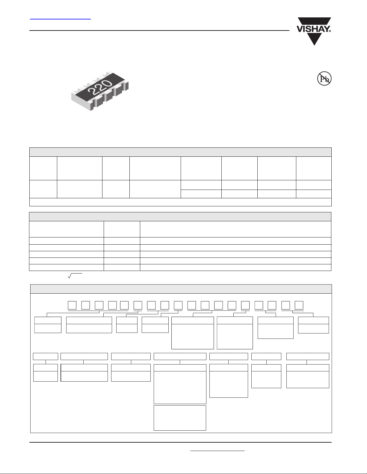
STANDARD ELECTRICAL SPECIFICATIONS
MODEL POWER RATING CIRCUIT LIMITING ELEMENT TEMPERATURE TOLERANCE RESISTANCE E-SERIES
P
70°C
WV쓖 ppm/K % Ω
CRA06P 0.0625 03 50
Jumper: Zero-Ohm-Resistor available; R ≤ 50m Ω
VOLTAGE MAX. COEFFICIENT RANGE
and lead containing soldering processes
• Compatible with "Restriction of the use of Hazardous
Substances" (RoHS) directive 2002/95/EC (issue 2004)
• Operating temperature range of -55°C to +150°C
200 ± 2; ± 5 10R - 1M0 24
100 ± 1 10R - 1M0 24 - 96
TECHNICAL SPECIFICATIONS
PARAMETER UNIT
Rated Dissipation at 70°C W 0.0625
Limiting Element Voltage
Insulation Voltage (1min) V
Category Temperature Range °C - 55 to + 150
Insulation Resistance Ω > 10
1) Rated voltage: P*R
1)
V쓖 50
dc/ac peak
CRA06P
03 CIRCUIT
100
PART NUMBER AND PRODUCT DESCRIPTION
PART NUMBER: CRA06P08310K0JTA
CRA06 P0 83 10 K0JT A
MODEL
CRA06
PRODUCT DESCRIPTION: CRA06P 08 03 473 J RT1 e3
CRA06P
MODEL
CRA06P
1)
Please refer to table PACKING, page 10.
NOTE: Products can be ordered using either the Product Description or the Part Number.
TERMINAL STYLE PIN
P
08
TERMINAL COUNT
08
08
03
CIRCUIT TYPE
03
CIRCUIT
3 = 03
RESISTANCE VALUE
4702 = 47KΩ
000 = 0Ω Jumper
First two digits (three
for 1 %) are significant.
Last digit is the
VALUE
R = Decimal
K = Thousand
M = Million
0000 = 0Ω Jumper
473 J
473 = 47KΩ
10R0 = 10Ω
100 = 10Ω
multiplier
TOLERANCE
F = ± 1%
G = ± 2%
J = ± 5%
Z = 0Ω Jumper
TOLERANCE
F = ± 1%
G = ± 2%
J = ± 5%
Z = 0Ω Jumper
10
PACKING
TA = RT1
TC = RT6
RT1
PACKING
RT1
RT6
1)
SPECIAL
up to 2 digits
e3
LEAD (Pb)-FREE
e3 = Pure Tin
Termination Finish
www.vishay.com
8
For Technical Questions, contact: ff3aresistors@vishay.com
Document Number 31047
Revision 25-Jul-05
Page 2
CRA06P
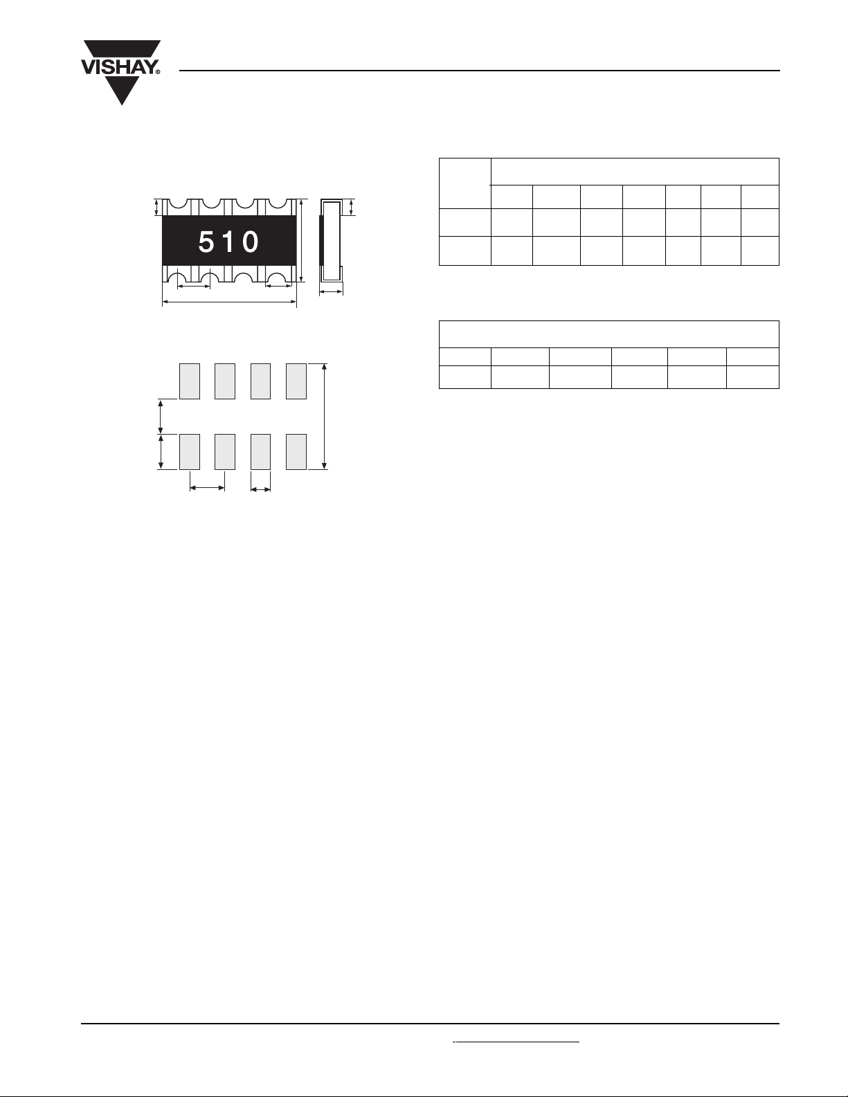
DIMENSIONS
4-Resistor Device
A
c
b
Thick Film, Resistor Array
PIN
NO#
C
8 3.20 0.30 0.40 0.40 0.80 0.60 1.6
w
P
L
B
T
w
Tol ± 0.20 ± 0.20 ± 0.15 ± 0.20 - ± 0.10 ± 0.15
WAVE 0.8 2.6 0.8 0.4 0.9
L ABCPTW
SOLDER PAD DIMENSIONS [in millimeters]
DIMENSIONS [in millimeters]
cwpab
Vishay Dale
p
a
DESCRIPTION
Production is strictly controlled and follows a set of instructions
established for reproducibility. A thick film layer is deposited
on a high grade ceramic substrate. The resistor elements are
covered by a protective coating designed for electrical,
mechanical and climatic protection. The wrap around
terminations receive a final pure tin on nickel plating.
The result of the determined production is verified by an
extensive testing procedure. Only accepted products are laid
directly into the paper tape in accordance with EIA 481.
ASSEMBLY
The resistors are suitable for processing on automatic SMD
assembly systems. They are suitable for automatic soldering
using wave and solder paste reflow. Due to the design, arrays
have automatic placement capability. The resistors are Lead
(Pb)-free, the pure tin plating provides compatibility with Lead
(Pb)-free and Lead-containing soldering processes. All
products comply with the CEFIC-EECA-EICTA list of legal
restrictions on hazardous substances.
This includes full compatibility with the following directives:
• 2000/53/EC End of Vehicle Life Directive (ELV)
• 2000/53/EC Annex II to End of Vehicle Life Directive (ELV II)
• 2002/95/EC Restriction of the use of Hazardous
Substances Directive (RoHS)
• 2002/96/EC Waste Electrical and Electronic Equipment
Directive (WEEE)
Document Number 31047
Revision 25-Jul-05
Solderability is specified for 2 years after production or re-
qualification. The permitted storage time is 20 years.
For Technical Questions, contact: ff3aresistors@vishay.com
www.vishay.com
9
Page 3

CRA06P
Vishay Dale
CIRCUIT
Thick Film, Resistor Array
03 Circuit
8-pin
120
100
Rated Power %
80
60
40
20
0
-55 -25 0 25 50 75 100 125 150
Derating
70
Ambient Temperature °C
PACKING
MODEL TAPE WIDTH DIAMETER PIECES PITCH
CRA06P
8 mm 180 mm/7" 5 000 4 mm RT1
8 mm 330 mm/13" 20 000 4 mm RT6
PACKING CODE
PAPER TAPE
www.vishay.com
10
For Technical Questions, contact: ff3aresistors@vishay.com
Document Number 31047
Revision 25-Jul-05
Page 4

CRA06P
Thick Film, Resistor Array
Vishay Dale
PERFORMANCE
TEST CONDITIONS OF TEST TEST RESULTS
Endurance Test at 70°C
per EIA 575-3.14
Overload
per EIA 575-3.6
Thermal Shock per EIA 575-3.5 ± 0.5 %
Moisture Resistance per EIA 575-3.10 ± 1.0 %
Resistance to Soldering Heat
EIA 575 3.8
High Temperature Exposure per EIA 575-3.7 ± 1.0 %
Low Temperature Operation per EIA-/ IS-30A-3.6 ± 0.5 %
Solderability & Leaching EIA 575-3.12 95 % Coverage
1000 hours at 70°C, 1.5 hours "ON", 0.5 hours "OFF" ± 1.0 %
Short time overload ± 0.5 %
10 seconds at 260°C solder bath temperature ± 1.0 %
Document Number 31047
Revision 25-Jul-05
For Technical Questions, contact: ff3aresistors@vishay.com
www.vishay.com
11
 Loading...