

www.vishay.com
IMS-2
IGBT SIP Module
(Ultrafast IGBT)
PRODUCT SUMMARY
OUTPUT CURRENT IN A TYPICAL 20 kHz MOTOR DRIVE
per phase (2.1 kW total)
I
RMS
with T
= 90 °C
C
T
J
Supply voltage 360 V
Power factor 0.8
Modulation depth (see fig. 1) 115 %
(typical)
V
CE(on)
at I
= 6.8 A, 25 °C
C
Package SIP
Circuit Three Phase Inverter
7.1 A
125 °C
1.7 V
RMS
DC
CPV363M4UPbF
Vishay Semiconductors
FEATURES
• Fully isolated printed circuit board mount
package
• Switching-loss rating includes all “tail” losses
•HEXFRED® soft ultrafast diodes
• Optimized for medium speed 1 to 10 kHz
See fig. 1 for current vs. frequency curve
• UL approved file E78996
• Designed and qualified for industrial level
• Material categorization: For definitions of compliance
please see www.vishay.com/doc?99912
DESCRIPTION
The IGBT technology is the key to Vishay’s Semiconductors
advanced line of IMS (Insulated Metal Substrate) power
modules. These modules are more efficient than
comparable bipolar transistor modules, while at the same
time having the simpler gate-drive requirements of the
familiar power MOSFET. This superior technology has now
been coupled to a state of the art materials system that
maximizes power throughput with low thermal resistance.
This package is highly suited to motor drive applications and
where space is at a premium.
RoHS
COMPLIANT
ABSOLUTE MAXIMUM RATINGS
PARAMETER SYMBOL TEST CONDITIONS MAX. UNITS
Collector to emitter voltage V
Continuous collector current, each IGBT I
Pulsed collector current I
Clamped inductive load current I
Diode continuous forward current I
Diode maximum forward current I
Gate to emitter voltage V
Isolation voltage V
Maximum power dissipation, each IGBT P
Operating junction and storage temperature range T
Soldering temperature For 10 s, (0.063" (1.6 mm) from case) 300
Mounting torque 6-32 or M3 screw
Notes
(1)
Repetitive rating; VGE = 20 V, pulse width limited by maximum junction temperature (see fig. 20)
(2)
VCC = 80 % (V
Revision: 11-Jun-13
For technical questions within your region: DiodesAmericas@vishay.com
THIS DOCUMENT IS SUBJECT TO CHANGE WITHOUT NOTICE. THE PRODUCTS DESCRIBED HEREIN AND THIS DOCUMENT
), VGE = 20 V, L = 10 μH, RG = 23 (see fig. 19)
CES
ARE SUBJECT TO SPECIFIC DISCLAIMERS, SET FORTH AT www.vishay.com/doc?91000
CM
LM
J
CES
C
F
FM
GE
ISOL
, T
TC = 25 °C 13
= 100 °C 6.8
T
C
(1)
(2)
TC = 100 °C 6.1
Any terminal to case, t = 1 min 2500 V
TC = 25 °C 36
D
T
= 100 °C 14
C
Stg
1
, DiodesAsia@vishay.com, DiodesEurope@vishay.com
600 V
40
40
40
± 20 V
- 40 to + 150
5 to 7
(0.55 to 0.8)
Document Number: 94486
lbf in
(N m)
A
RMS
W
°C
CPV363M4UPbF
www.vishay.com
THERMAL AND MECHANICAL SPECIFICATIONS
PARAMETER SYMBOL TYP. MAX. UNITS
Junction to case, each IGBT, one IGBT in conduction R
Case to sink, flat, greased surface R
Weight of module
(IGBT) - 3.5
thJC
(DIODE) - 5.5
thJC
(MODULE) 0.10 -
thCS
20 - g
0.7 - oz.
ELECTRICAL SPECIFICATIONS (TJ = 25 °C unless otherwise specified)
PARAMETER SYMBOL TEST CONDITIONS MIN. TYP. MAX. UNITS
(1)
Collector to emitter breakdown voltage V
Temperature coeff. of breakdown
voltage
Collector to emitter saturation voltage V
Gate threshold voltage V
Temperature coeff. of threshold voltage V
Forward transconductance g
Zero gate voltage collector current I
Diode forward voltage drop V
Gate to emitter leakage current I
Notes
(1)
Pulse width 80 μs, duty factor 0.1 %
(2)
Pulse width 5.0 μs; single shot
V
(BR)CES
(BR)CES
CE(on)
GE(th)
GE(th)
fe
CES
FM
GES
/T
(2)
VGE = 0 V, IC = 250 μA 600 - - V
TJVGE = 0 V, IC = 1.0 mA - 0.63 - V/°C
IC = 6.8 A
V
= 15 V
= 13 A - 2.00 -
I
C
= 6.8 A, TJ = 150 °C - 1.70 -
I
C
GE
See fig. 2, 5
VCE = VGE, IC = 250 μA
J
VCE = 100 V, IC = 6.8 A 4.0 6.0 - S
VGE = 0 V, VCE = 600 V - - 250
V
= 0 V, VCE = 600 V, TJ = 150 °C - - 2500
GE
IC = 12 A
I
= 12 A, TJ = 150 °C - 1.3 1.6
C
See fig. 13
VGE = ± 20 V - - ± 100 nA
Vishay Semiconductors
°C/WJunction to case, each DIODE, one DIODE in conduction R
- 1.70 2.2
3.0 - 6.0
-- 11-mV/°C
-1.41.7
V
μA
V
Revision: 11-Jun-13
For technical questions within your region: DiodesAmericas@vishay.com
2
, DiodesAsia@vishay.com, DiodesEurope@vishay.com
Document Number: 94486
THIS DOCUMENT IS SUBJECT TO CHANGE WITHOUT NOTICE. THE PRODUCTS DESCRIBED HEREIN AND THIS DOCUMENT
ARE SUBJECT TO SPECIFIC DISCLAIMERS, SET FORTH AT www.vishay.com/doc?91000
CPV363M4UPbF
www.vishay.com
SWITCHING CHARACTERISTICS (TJ = 25 °C unless otherwise specified)
PARAMETER SYMBOL TEST CONDITIONS MIN. TYP. MAX. UNITS
Total gate charge (turn-on) Q
Gate to collector charge (turn-on) Q
Turn-on delay time t
Rise time t
Turn-off delay time t
Fall time t
Turn-on switching loss E
Total switching loss E
Turn-on delay time t
Rise time t
Turn-off delay time t
Fall time t
Total switching loss E
Input capacitance C
Reverse transfer capacitance C
Diode reverse recovery time t
Diode peak reverse recovery charge I
Diode reverse recovery charge Q
Diode peak rate of fall of recovery
during t
b
dI
d(on)
d(off)
d(on)
d(off)
oes
(rec)M
on
off
ies
res
rr
rr
g
ge
gc
r
f
IC = 6.8 A
= 400 V
V
CC
See fig. 8
TJ = 25 °C
I
= 6.8 A, VCC = 480 V
C
V
= 15 V, RG = 23
GE
Energy losses include “tail” and diode
reverse recovery.
See fig. 9, 10, 11, 18
ts
TJ = 150 °C
I
= 6.8 A, VCC = 480 V
r
C
V
= 15 V, RG = 23
GE
Energy losses include “tail” and
f
ts
diode reverse recovery
See fig. 9, 10, 11, 18
VGE = 0 V
V
= 30 V
CC
ƒ = 1.0 MHz
See fig. 7
TJ = 25 °C
T
= 125 °C - 83 120
J
TJ = 25 °C
T
= 125 °C - 5.6 10
J
TJ = 25 °C
rr
/dt
T
= 125 °C - 220 600
J
= 25 °C
T
J
T
= 125 °C - 116 -
J
See fig. 14
See fig. 15
See fig. 16
See fig. 17
I
= 12 A
F
V
= 200 V
R
dI/dt = 200 A/μs
Vishay Semiconductors
-5379
-7.712
-2131
-43-
-14-
- 95 140
- 83 190
-0.17-
-0.15-
- 0.32 0.45
-41-
-16-
-110-
-230-
-0.52-mJ
- 1100 -
-73-
-14-
-4260
-3.56.0
- 80 180
-180-
nCGate to emitter charge (turn-on) Q
ns
mJTurn-off switching loss E
ns
pFOutput capacitance C
ns
A
nC
A/μs
Revision: 11-Jun-13
For technical questions within your region: DiodesAmericas@vishay.com
3
, DiodesAsia@vishay.com, DiodesEurope@vishay.com
Document Number: 94486
THIS DOCUMENT IS SUBJECT TO CHANGE WITHOUT NOTICE. THE PRODUCTS DESCRIBED HEREIN AND THIS DOCUMENT
ARE SUBJECT TO SPECIFIC DISCLAIMERS, SET FORTH AT www.vishay.com/doc?91000
www.vishay.com
0.1 1 10 100
0
2
4
6
8
10
12
f, Frequency (KHz)
LOAD CURRENT (A)
Tc = 90°C
Tj = 125°C
Power Factor = 0.8
Modulation Depth = 1.15
Vcc = 50% of Rat ed Voltage
0.00
0.58
1.17
1.75
2.33
2.92
3.50
Total Output Power (kW)
0.1
1
10
100
5678910
C
I , Collector-to-Emitter Current (A)
GE
T = 25°C
T = 150°C
J
J
V , Gate-to-Emitter Voltage (V)
V = 10V
5µs PULSE WIDTH
CC
-60 -40 -20 0 20 40 60 80 100 120 140 160
1.0
2.0
3.0
T , Junction Temperature ( C)
V , Collector-to-Emitter Voltage(V)
J
°
CE
V = 15V
80 us PULSE W IDTH
GE
I = A3.4
C
I = A
6.8
C
I = A
13.6
C
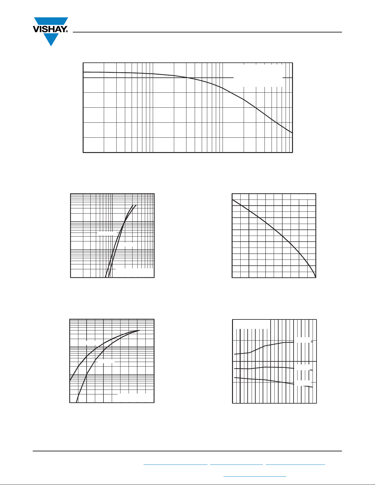
Fig. 1 - Typical Load Current vs. Frequency
(Load Current = I
of Fundamental)
RMS
CPV363M4UPbF
Vishay Semiconductors
100
10
T = 150°C
J
T = 25°C
1
C
I , Collector-to-Emitter Current (A)
0.1
V , Collector-to-Emitter Voltage (V)
CE
J
V = 15V
GE
20µs PULSE WIDTH
Fig. 2 - Typical Output Characteristics
14
12
10
8
6
4
2
Maximum DC Collector Current (A)
0111.0
0
25 50 75 100 125 150
T , Case Temperature (°C)
C
V = 15V
GE
Fig. 4 - Maximum Collector Current vs. Case Temperature
Revision: 11-Jun-13
For technical questions within your region: DiodesAmericas@vishay.com
THIS DOCUMENT IS SUBJECT TO CHANGE WITHOUT NOTICE. THE PRODUCTS DESCRIBED HEREIN AND THIS DOCUMENT
Fig. 3 - Typical Transfer Characteristics
ARE SUBJECT TO SPECIFIC DISCLAIMERS, SET FORTH AT www.vishay.com/doc?91000
4
Fig. 5 - Typical Collector to Emitter Voltage vs.
Junction Temperature
Document Number: 94486
, DiodesAsia@vishay.com, DiodesEurope@vishay.com

www.vishay.com
0.01
0.1
1
10
0.00001 0.0001 0.001 0.01 0.1 1 10
t , Rectangular Pulse Duration (sec)
1
thJC
D = 0.50
0.01
0.02
0.05
0.10
0.20
SI NGLE PULSE
(THERMAL RESPONSE)
Thermal Response (Z )
P
t
2
1
t
DM
Notes:
1. Duty factor D = t / t
2. Peak T = P x Z + T
12
J
DM
thJC
C
0 10 20 30 40 50 60
0
4
8
12
16
20
Q , Total Gate Charge (nC)
V , Gate-to-Emitter Voltage (V)
G
GE
V = 400V
I = 6.8A
CC
C
Fig. 6 - Maximum Effective Transient Thermal Impedance, Junction to Case
CPV363M4UPbF
Vishay Semiconductors
2000
1600
1200
800
V = 0V, f = 1MHz
GE
C = C + C , C SHORTED
ies ge gc c e
C = C
res gc
C = C + C
oes ce gc
C
ies
C
oes
C, Capacitance (pF)
C
400
res
0
V , Collector-to-Emitter Voltage (V)
CE
001011
Fig. 7 - Typical Capacitance vs. Collector to Emitter Voltage
0.40
V = 480V
CC
V = 15V
GE
°
T = 25 C
J
I = 6.8A
0.38
C
0.36
0.34
0.32
Total Switching Losses (mJ)
0.30
0 12 24 36 48 60
R , Gate Resistance ( )
G
Ω
Fig. 9 - Typical Switching Losses vs. Gate Resistance
10
R = 23
V = 15V
V = 480V
1
GE
CC
Ω
G
I = A
13.6
C
Fig. 8 - Typical Gate Charge vs. Gate to Emitter Voltage
Revision: 11-Jun-13
For technical questions within your region: DiodesAmericas@vishay.com
THIS DOCUMENT IS SUBJECT TO CHANGE WITHOUT NOTICE. THE PRODUCTS DESCRIBED HEREIN AND THIS DOCUMENT
Fig. 10 - Typical Switching Losses vs. Junction Temperature
5
, DiodesAsia@vishay.com, DiodesEurope@vishay.com
ARE SUBJECT TO SPECIFIC DISCLAIMERS, SET FORTH AT www.vishay.com/doc?91000
I = A
C
I = A
Total Switching Losses (mJ)
0.1
-60 -40 -20 0 20 40 60 80 100 120 140 160
T , Junction Temperature ( C )
J
C
°
Document Number: 94486
6.8
3.4

www.vishay.com
0 2 4 6 8 10 12 14 16
0.0
0.2
0.4
0.6
0.8
1.0
1.2
I , Collector-to-emitter Current (A)
Total Switching Losses (mJ)
C
R = 23
T = 150 C
V = 480V
V = 15V
G
J
CC
GE
°
Ω
Fig. 11 - Typical Switching Losses vs.
Collector to Emitter Current
100
CPV363M4UPbF
Vishay Semiconductors
100
V = 20V
GE
T = 125 C
10
1
C
I , Collector-to-Emitter Current (A)
0.1
1 10 100 1000
o
J
SAFE OPERATING AREA
V , Collector-to-Emitter Voltage (V)
CE
Fig. 12 - Turn-Off SOA
F
T = 150°C
J
T = 125°C
10
J
T = 25°C
J
Instantaneous Forward Current - I (A)
1
0.4 1.4 2.4
Forward Voltage Drop - V (V)
FM
Fig. 13 - Maximum Forward Voltage Drop vs.
Instantaneous Forward Current
Revision: 11-Jun-13
For technical questions within your region: DiodesAmericas@vishay.com
THIS DOCUMENT IS SUBJECT TO CHANGE WITHOUT NOTICE. THE PRODUCTS DESCRIBED HEREIN AND THIS DOCUMENT
6
, DiodesAsia@vishay.com, DiodesEurope@vishay.com
ARE SUBJECT TO SPECIFIC DISCLAIMERS, SET FORTH AT www.vishay.com/doc?91000
Document Number: 94486

www.vishay.com
1
10
100
0001001
f
di /dt - (A/µs)
I - (A)
IRRM
I = 6.0A
I = 12A
I = 24A
F
F
F
V = 200V
T = 125°C
T = 25 °C
R
J
J
0
200
400
600
0001001
f
di /dt - (A/µs)
RR
Q - (nC)
I = 6.0A
I = 12A
I = 24A
V = 200V
T = 12 5°C
T = 25 °C
R
J
J
F
F
F
160
120
80
rr
t - (ns)
40
I = 24A
F
V = 200V
R
T = 125°C
J
T = 25 °C
J
I = 12A
F
I = 6.0A
F
CPV363M4UPbF
Vishay Semiconductors
0
di /dt - (A/µs)
f
Fig. 14 - Typical Reverse Recovery Time vs. dIF/dt
Fig. 15 - Typical Recovery Current vs. dI
/dt
F
0001001
Fig. 16 - Typical Stored Charge vs. dI
10000
V = 200V
R
T = 12 5°C
J
T = 25 °C
J
1000
100
di(rec)M/dt - (A/µs)
10
Fig. 17 - Typical dI
I = 6.0A
F
I = 24A
F
di /dt - (A/µs)
f
(rec)M
I = 12A
/dt vs dIF/dt
F
/dt
F
0001001
Revision: 11-Jun-13
THIS DOCUMENT IS SUBJECT TO CHANGE WITHOUT NOTICE. THE PRODUCTS DESCRIBED HEREIN AND THIS DOCUMENT
7
For technical questions within your region: DiodesAmericas@vishay.com
ARE SUBJECT TO SPECIFIC DISCLAIMERS, SET FORTH AT www.vishay.com/doc?91000
Document Number: 94486
, DiodesAsia@vishay.com, DiodesEurope@vishay.com

www.vishay.com
Same type
device as
D.U.T.
D.U.T.
430 µF
80 %
of V
CE
t1
Ic
Vce
t1
t2
90% Ic
10% Vce
td(off)
tf
Ic
5% Ic
t1+5µS
Vce ic dt
90% Vge
+Vge
∫
Eoff =
DIODE REVERSE
RECOV ERY ENER GY
tx
∫
Erec =
t4
t3
Vd id dt
t4
t3
DIODE RE COVERY
WAVEFORMS
Ic
Vpk
10% Vcc
Irr
10% Irr
Vcc
trr
∫
Qrr =
trr
tx
id dt
10% +Vg
CPV363M4UPbF
Vishay Semiconductors
GATE VOLTAG E D.U.T.
+Vg
Fig. 18a - Test Circuit for Measurements of ILM, Eon, E
I
, t
, tr, t
rr
d(on)
d(off)
, t
f
off(diode)
, trr, Qrr,
DUT VOLTAGE
AND CURR ENT
Ipk
Ic
t2
Vce ie dt
Eon =
∫
t1
t2
Vcc
10% Ic
td(on)
Vce
90% Ic
5% Vce
tr
t1
Fig. 18c - Test Waveforms for Circuit of Fig. 18a,
Defining E
, t
, t
on
d(on)
r
Fig. 18b - Test Waveforms for Circuit of Fig. 18a,
Defining E
Revision: 11-Jun-13
For technical questions within your region: DiodesAmericas@vishay.com
THIS DOCUMENT IS SUBJECT TO CHANGE WITHOUT NOTICE. THE PRODUCTS DESCRIBED HEREIN AND THIS DOCUMENT
, t
, t
off
d(off)
f
Vg
t0
t1
t2
Fig. 18e - Macro Waveforms for Figure 18a’s Test Circuit
8
Fig. 18d - Test Waveforms for Circuit of Fig. 18a,
GATE SIGNAL
DEVIC E UNDER TE S
CURRENT D.U.T.
VOLTAGE IN D.U.T.
CURRENT IN D1
Defining E
, trr, Qrr, I
rec
Document Number: 94486
, DiodesAsia@vishay.com, DiodesEurope@vishay.com
ARE SUBJECT TO SPECIFIC DISCLAIMERS, SET FORTH AT www.vishay.com/doc?91000
rr

www.vishay.com
D.U.T.
50 V
6000 µF
100 V
1000 V
L
V
C
0 - 480 V
R
L
=
480 V
4 x I
C
at 25 °C
Fig. 19 - Clamped Inductive Load Test Circuit Fig. 20 - Pulsed Collector Current Test Circuit
CIRCUIT CONFIGURATION
CPV363M4UPbF
Vishay Semiconductors
1
Q1
3
Q2
618
71319
Q3D1
9
41016
D2
12
D3
D4
Q5
15
Q6
D5
D6Q4
LINKS TO RELATED DOCUMENTS
Dimensions www.vishay.com/doc?95066
Revision: 11-Jun-13
For technical questions within your region: DiodesAmericas@vishay.com
THIS DOCUMENT IS SUBJECT TO CHANGE WITHOUT NOTICE. THE PRODUCTS DESCRIBED HEREIN AND THIS DOCUMENT
9
, DiodesAsia@vishay.com, DiodesEurope@vishay.com
ARE SUBJECT TO SPECIFIC DISCLAIMERS, SET FORTH AT www.vishay.com/doc?91000
Document Number: 94486

DIMENSIONS in millimeters (inches)
IMS-2 Package Outline (13 Pins)
7.87 (0.310)
5.46 (0.215)
1.27 (0.050)
6.10 (0.240)
3.05 ± 0.38
(0.120 ± 0.015)
0.51 (0.020)
0.38 (0.015)
62.43 (2.458)
53.85 (2.120)
Ø 3.91 (0.154)
2 x
21.97 (0.865)
3.94 (0.155)
4.06 ± 0.51
(0.160 ± 0.020)
5.08 (0.200)
6 x
1.27 (0.050)
13 x
2.54 (0.100)
6 x
0.76 (0.030)
13 x
1 3 4 6 7 9 10 12 13 15 16 18 19171411258
Outline Dimensions
Vishay Semiconductors
IMS-2 (SIP)
Notes
(1)
Tolerance uless otherwise specified ± 0.254 mm (0.010")
(2)
Controlling dimension: inch
(3)
Terminal numbers are shown for reference only
Document Number: 95066 For technical questions, contact: indmodules@vishay.com
Revision: 30-Jul-07 1
www.vishay.com

Legal Disclaimer Notice
www.vishay.com
Vishay
Disclaimer
ALL PRODUCT, PRODUCT SPECIFICATIONS AND DATA ARE SUBJECT TO CHANGE WITHOUT NOTICE TO IMPROVE
RELIABILITY, FUNCTION OR DESIGN OR OTHERWISE.
Vishay Intertechnology, Inc., its affiliates, agents, and employees, and all persons acting on its or their behalf (collectively,
“Vishay”), disclaim any and all liability for any errors, inaccuracies or incompleteness contained in any datasheet or in any other
disclosure relating to any product.
Vishay makes no warranty, representation or guarantee regarding the suitability of the products for any particular purpose or
the continuing production of any product. To the maximum extent permitted by applicable law, Vishay disclaims (i) any and all
liability arising out of the application or use of any product, (ii) any and all liability, including without limitation special,
consequential or incidental damages, and (iii) any and all implied warranties, including warranties of fitness for particular
purpose, non-infringement and merchantability.
Statements regarding the suitability of products for certain types of applications are based on Vishay’s knowledge of typical
requirements that are often placed on Vishay products in generic applications. Such statements are not binding statements
about the suitability of products for a particular application. It is the customer’s responsibility to validate that a particular
product with the properties described in the product specification is suitable for use in a particular application. Parameters
provided in datasheets and/or specifications may vary in different applications and performance may vary over time. All
operating parameters, including typical parameters, must be validated for each customer application by the customer’s
technical experts. Product specifications do not expand or otherwise modify Vishay’s terms and conditions of purchase,
including but not limited to the warranty expressed therein.
Except as expressly indicated in writing, Vishay products are not designed for use in medical, life-saving, or life-sustaining
applications or for any other application in which the failure of the Vishay product could result in personal injury or death.
Customers using or selling Vishay products not expressly indicated for use in such applications do so at their own risk. Please
contact authorized Vishay personnel to obtain written terms and conditions regarding products designed for such applications.
No license, express or implied, by estoppel or otherwise, to any intellectual property rights is granted by this document or by
any conduct of Vishay. Product names and markings noted herein may be trademarks of their respective owners.
Material Category Policy
Vishay Intertechnology, Inc. hereby certifies that all its products that are identified as RoHS-Compliant fulfill the
definitions and restrictions defined under Directive 2011/65/EU of The European Parliament and of the Council
of June 8, 2011 on the restriction of the use of certain hazardous substances in electrical and electronic equipment
(EEE) - recast, unless otherwise specified as non-compliant.
Please note that some Vishay documentation may still make reference to RoHS Directive 2002/95/EC. We confirm that
all the products identified as being compliant to Directive 2002/95/EC conform to Directive 2011/65/EU.
Vishay Intertechnology, Inc. hereby certifies that all its products that are identified as Halogen-Free follow Halogen-Free
requirements as per JEDEC JS709A standards. Please note that some Vishay documentation may still make reference
to the IEC 61249-2-21 definition. We confirm that all the products identified as being compliant to IEC 61249-2-21
conform to JEDEC JS709A standards.
Revision: 02-Oct-12
1
Document Number: 91000
 Loading...