

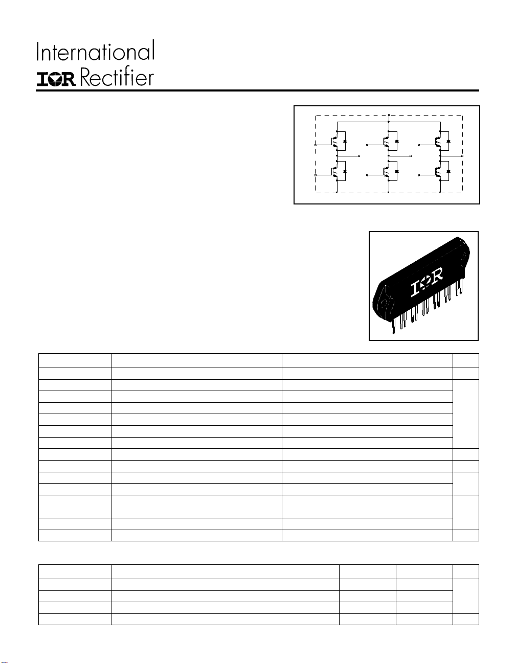
CPV362M4F
Features
• Fully isolated printed circuit board mount package
• Switching-loss rating includes all "tail" losses
• HEXFRED
TM
soft ultrafast diodes
• Optimized for medium operating (1 to 10 kHz)
See Fig. 1 for Current vs. Frequency curve
Product Summary
Output Current in a Typical 5.0 kHz Motor Drive
11 A
per phase (3.1 kW total) with TC = 90°C, TJ = 125°C, Supply Voltage 360Vdc,
RMS
Power Factor 0.8, Modulation Depth 115% (See Figure 1)
Description
The IGBT technology is the key to International Rectifier's advanced line of
IMS (Insulated Metal Substrate) Power Modules. These modules are more
efficient than comparable bipolar transistor modules, while at the same time
having the simpler gate-drive requirements of the familiar power MOSFET.
This superior technology has now been coupled to a state of the art materials
system that maximizes power throughput with low thermal resistance. This
package is highly suited to motor drive applications and where space is at a
premium.
Q1
3
Q2
6
71319
PD -5.046
Fast IGBTIGBT SIP MODULE
1
D1 D3 D5
Q3
9
D2 D4 D6
Q4
12
15
18
Q5
10 164
Q6
IMS-2
Absolute Maximum Ratings
Parameter Max. Units
V
CES
Collector-to-Emitter Voltage 600 V
IC @ TC = 25°C Continuous Collector Current, each IGBT 8.8
@ TC = 100°C Continuous Collector Current, each IGBT 4.8
I
C
I
CM
I
LM
@ TC = 100°C Diode Continuous Forward Current 3.4
I
F
I
FM
V
GE
V
ISOL
Pulsed Collector Current 26 A
Clamped Inductive Load Current 26
Diode Maximum Forward Current 26
Gate-to-Emitter Voltage ±20 V
Isolation Voltage, any terminal to case, 1 minute 2500 V
RMS
PD @ TC = 25°C Maximum Power Dissipation, each IGBT 23 W
@ TC = 100°C Maximum Power Dissipation, each IGBT 9.1
P
D
T
J
T
STG
Operating Junction and -40 to +150
Storage Temperature Range °C
Soldering Temperature, for 10 sec. 300 (0.063 in. (1.6mm) from case)
Mounting torque, 6-32 or M3 screw 5-7 lbf•in (0.55-0.8 N•m)
Thermal Resistance
Parameter Typ. Max. Units
R
(IGBT) Junction-to-Case, each IGBT, one IGBT in conduction ––– 5.5
θJC
R
(DIODE) Junction-to-Case, each diode, one diode in conduction ––– 9.0 °C/W
θJC
(MODULE) Case-to-Sink, flat, greased surface 0.1 –––
R
θCS
Wt Weight of module 20 (0.7) ––– g (oz)
9/16/97
CPV362M4F
Electrical Characteristics @ TJ = 25°C (unless otherwise specified)
Parameter Min. Typ. Max. Units Conditions
V
(BR)CES
∆V
(BR)CES
V
CE(on)
V
GE(th)
∆V
GE(th)
g
fe
I
CES
V
FM
I
GES
Switching Characteristics @ TJ = 25°C (unless otherwise specified)
Parameter Min. Typ. Max. Units Conditions
Q
g
Q
ge
Q
gc
t
d(on)
t
r
t
d(off)
t
f
E
on
E
off
E
ts
t
d(on)
t
r
t
d(off)
t
f
E
ts
C
ies
C
oes
C
res
t
rr
I
rr
Q
rr
di
(rec)M
Notes:
Repetitive rating; V
Collector-to-Emitter Breakdown Voltage 600 ––– ––– V VGE = 0V, IC = 250µA
/∆T
Temperature Coeff. of Breakdown Voltage – – – 0.72 ––– V/°C VGE = 0V, IC = 1.0mA
J
Collector-to-Emitter Saturation Voltage –– – 1.41 1.7 IC = 4.8A VGE = 15V
––– 1.66 ––– V I
= 8.8A See Fig. 2, 5
C
––– 1.42 ––– IC = 4.8A, TJ = 150°C
Gate Threshold Voltage 3.0 –– – 6. 0 VCE = VGE, IC = 250µA
/∆TJTemperature Coeff. of Threshold Voltage –– – - 1 1 – – – mV/°C VCE = VGE, IC = 250µA
Forward Transconductance 2.9 5.0 ––– S VCE = 100V, IC = 4.8A
Zero Gate Voltage Collector Current ––– ––– 250 µA VGE = 0V, VCE = 600V
––– ––– 1700 VGE = 0V, VCE = 600V, TJ = 150°C
Diode Forward Voltage Drop –– – 1.4 1.7 V IC = 8.0A See Fig. 13
––– 1.3 1.6 I
= 8.0A, TJ = 150°C
C
Gate-to-Emitter Leakage Current ––– ––– ±100 nA VGE = ±20V
Total Gate Charge (turn-on) ––– 30 45 IC = 4.8A
Gate - Emitter Charge (turn-on) ––– 4.0 6.0 nC VCC = 400V
Gate - Collector Charge (turn-on) ––– 13 20 See Fig. 8
Turn-On Delay Time ––– 49 ––– TJ = 25°C
Rise Time ––– 22 ––– ns IC = 4.8A, VCC = 480V
Turn-Off Delay Time ––– 200 300 VGE = 15V, RG = 50Ω
Fall Time ––– 214 320 Energy losses include "tail" and
Turn-On Switching Loss ––– 0.23 ––– diode reverse recovery
Turn-Off Switching Loss ––– 0.33 ––– mJ See Fig. 9, 10, 18
Total Switching Loss ––– 0.45 0.70
Turn-On Delay Time ––– 48 ––– TJ = 150°C, See Fig. 10,11, 18
Rise Time ––– 25 ––– ns IC = 4.8A, VCC = 480V
Turn-Off Delay Time ––– 435 ––– VGE = 15V, RG = 50Ω
Fall Time ––– 364 ––– Energy losses include "tail" and
Total Switching Loss ––– 0.93 ––– mJ diode reverse recovery
Input Capacitance ––– 340 ––– VGE = 0V
Output Capacitance ––– 63 ––– pF VCC = 30V See Fig. 7
Reverse Transfer Capacitance ––– 5.9 ––– ƒ = 1.0MHz
Diode Reverse Recovery Time ––– 37 55 ns TJ = 25°C See Fig.
––– 55 90 TJ = 125°C 14 IF = 8.0A
Diode Peak Reverse Recovery Current ––– 3 .5 50 A TJ = 25°C See Fig.
––– 4.5 8.0 T
= 125°C 15 VR = 200V
J
Diode Reverse Recovery Charge ––– 65 138 nC TJ = 25°C See Fig.
––– 124 360 T
= 125°C 16 di/dt = 200A/µs
J
/dt Diode Peak Rate of Fall of Recovery ––– 240 ––– A/µs TJ = 25°C See Fig.
During t
b
=20V, pulse width
GE
limited by max. junction temperature.
( See fig. 20 )
––– 210 ––– TJ = 125°C 17
V
=80%(V
CC
), VGE=20V, L=10µH,
CES
RG= 50Ω, ( See fig. 19 )
Pulse width ≤ 80µs; duty factor ≤ 0.1%.
Pulse width 5.0µs, single
shot.
CPV362M4F
9
8
7
6
5
4
3
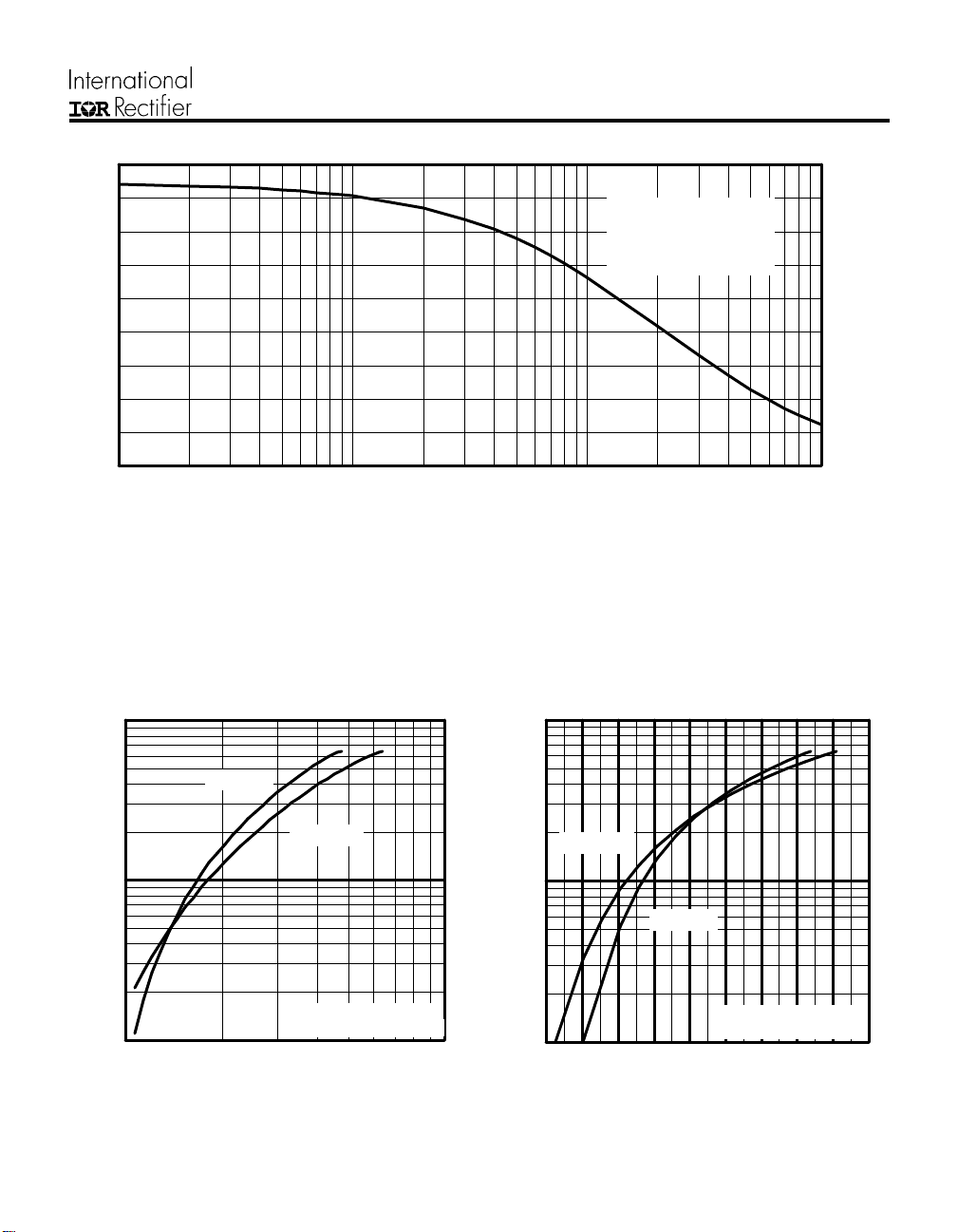
LOAD CURRENT (A)
2
1
0
0.1 1 10 100
Tc = 90°C
Tj = 125°C
Power Factor = 0.8
Modulation Depth = 1.15
Vcc = 50% of Rated Voltage
f, Frequency (KHz)
Fig. 1 - Typical Load Current vs. Frequency
(Load Current = I
of fundamental)
RMS
2.63
2.34
2.05
1.75
1.46
1.17
0.88
0.58
0.29
0.00
Total Output Power (kW)
100
o
T = 25 C
J
o
T = 150 C
J
10
C
I , Collector-to-Emitter Current (A)
1
1 10
V , Collector-to-Emitter Voltage (V)
CE
V = 15V
GE
20µs PULSE WIDTH
100
o
T = 150 C
J
10
o
T = 25 C
J
C
I , Collector-to-Emitter Current (A)
1
5 6 7 8 9 10 11 12 13 14
V , Gate-to-Emitter Voltage (V)
GE
V = 50V
CC
5µs PULSE WIDTH
Fig. 2 - Typical Output Characteristics Fig. 3 - Typical Transfer Characteristics

CPV362M4F
10
8
6
4
2
Maximum DC Collector Current(A)
0
25 50 75 100 125 150
°
T , Case Temperature ( C)
C
C)
Fig. 4 - Maximum Collector Current vs. Case
Temperature
10
2.5
V = 15V
GE
80 us PULSE WIDTH
I = A9.6
C
2.0
I = A4.8
C
1.5
I = A2.4
C
CE
V , Collector-to-Emitter Voltage(V)
1.0
-60 -40 -20 0 20 40 60 80 100 120 140 160
T , Junction Temperature ( C)
J
°
Fig. 5 - Typical Collector-to-Emitter Voltage
vs. Junction Temperature
D = 0.50
th JC
Th ermal Response (Z )
0.01
0.20
1
0.10
0.05
0.02
0.01
0.1
0.00001 0.0001 0.001 0.01 0.1 1 10
SINGLE PULSE
(THERMAL RESPONSE)
Notes:
1. Duty factor D = t / t
2. Peak T = P x Z + T
t , R ecta ng u lar Pu lse Dur a t ion ( sec )
1
J
DM
P
DM
12
thJC
t
1
t
2
C
Fig. 6 - Maximum Effective Transient Thermal Impedance, Junction-to-Case

CPV362M4F
1000
800
600
400
V
=
0V,
GE
C
=
ies ge gc , ce
C
=
res gc
C
=
oes ce gc
f = 1MHz
C
+ C
C
C
+ C
C
ies
C SHORTED
C, Capacitance (pF)
200
0
1 10 100
V , Collector-to-Emitter Voltage (V)
CE
C
oes
C
res
Fig. 7 - Typical Capacitance vs.
Collector-to-Emitter Voltage
0.46
V = 480V
CC
V = 15V
T = 25 C
0.45
GE
J
I = 4.8A
C
°
20
V = 400V
CC
I = 4.8A
C
16
12
8
4
GE
V , Gate-to-Emitter Voltage (V)
0
0 6 12 18 24 30
Q , Total Gate Charge (nC)
G
Fig. 8 - Typical Gate Charge vs.
Gate-to-Emitter Voltage
10
R = 50Ohm
50Ω
G
V = 15V
GE
V = 480V
CC
0.44
0.43
Total Switching Losses (mJ)
0.42
10 20 30 40 50
R , Gate Resistance (Ohm)
G
(Ω)
Fig. 9 - Typical Switching Losses vs. Gate
Resistance
I = A
C
1
I = A
C
I = A
C
Total Switching Losses (mJ)
0.1
-60 -40 -20 0 20 40 60 80 100 120 140 160
T , Junction Temperature ( C )
J
°
Fig. 10 - Typical Switching Losses vs.
Junction Temperature
9.6
4.8
2.4

CPV362M4F
2.0
R = 50Ohm
50 Ω
T = 150 C
V = 480V
CC
V = 15V
GE
1.5
1.0
0.5
G
J
°
Total Switching Losses (mJ)
0.0
0 2 4 6 8 10
I , Collector-to-emitter Current (A)
C
Fig. 11 - Typical Switching Losses vs.
Collector-to-Emitter Current
100
100
V = 20V
GE
GE
T = 125° C
J
SAFE O PERATING AREA
10
C
I , Co lle c t o r-to -Emitter Cu rr e n t (A )
1
1 10 100 1000
V , Co llec tor- to -E m i tte r V olta ge (V )
CE
Fig. 12 - Turn-Off SOA
F
10
T = 150°C
J
T = 125°C
J
T = 25°C
J
1
Instantaneous Forward Current - I (A)
0.1
0.4 0.8 1.2 1.6 2.0 2.4 2.8 3.2
Forward Voltage Drop - V (V)
FM
Fig. 13 - Maximum Forward Voltage Drop vs. Instantaneous Forward Current

CPV362M4F
100
V = 200V
R
T = 125°C
J
T = 25°C
J
80
I = 16A
F
60
rr
t - (ns )
40
I = 4.0A
F
20
0
100 1000
di /dt - ( A /µs)
f
I = 8.0 A
F
Fig. 14 - Typical Reverse Recovery vs. dif/dt
500
V = 200V
R
T = 125°C
J
T = 25°C
J
400
100
V = 200V
R
T = 125°C
J
T = 25°C
J
I = 16A
10
IRRM
I - (A )
I = 8.0A
F
1
100 1000
F
I = 4.0A
di /d t - ( A / µ s )
f
F
Fig. 15 - Typical Recovery Current vs. dif/dt
10000
V = 200V
R
T = 125°C
J
T = 25 °C
J
300
I = 4.0A
I = 16A
F
RR
Q - ( n C )
200
I = 8.0 A
F
100
0
100 1000
di / d t - ( A /µ s)
f
I = 4.0A
F
1000
di(re c )M /d t - (A / µ s )
100
100 1000
F
I = 8. 0A
F
I = 16A
F
di /d t - ( A /µ s )
Fig. 16 - Typical Stored Charge vs. dif/dt Fig. 17 - Typical di
f
(rec)M
/dt vs. dif/dt
CPV362M4F
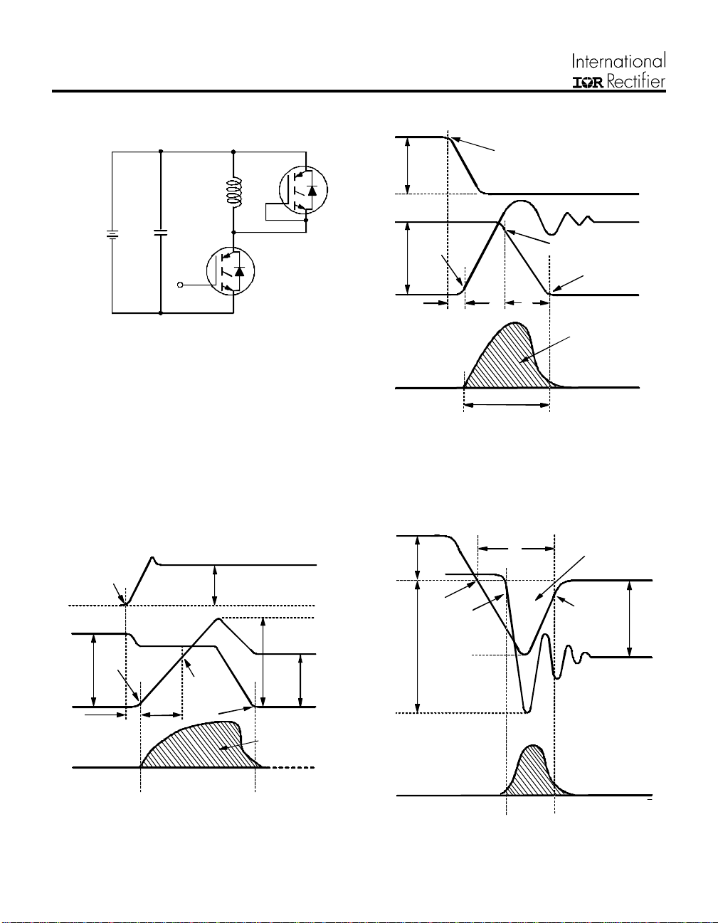
Same type
device as
D.U.T.
80%
of Vce
430µF
D.U.T.
Fig. 18a - Test Circuit for Measurement of
I
LM
Vcc
, Eon, E
10% +Vg
10% Ic
td(on)
t1 t2
off(diode)
Vce
tr
, trr, Qrr, Irr, t
GATE VOLTAGE D.U.T.
+Vg
90% Ic
5% Vce
d(on)
, tr, t
Eon =
, t
d(off)
DUT VOLTAGE
AND CURRENT
Ipk
Ic
t2
Vce ie dt
Vce Ic dt
∫
t1
90% Vge
+Vge
Vce
10% Vce
Ic
td(off)
f
t1
90% Ic
Ic
5% Ic
tf
Eoff =
t2
t1+5µS
Vce Ic dt
Vce ic dt
∫
t1
Fig. 18b - Test Waveforms for Circuit of Fig. 18a, Defining
, t
d(off)
t3
, t
f
trr
10% Irr
DIODE RE COV E RY
WAVEFORMS
Erec =
t4
Qrr =
∫
t3
trr
id dt
Ic dt
∫
tx
t4
Vd id dt
Vd Ic dt
Vcc
E
off
Ic
tx
10% Vcc
Vpk
DIODE REVERSE
RECOVERY ENERGY
Irr
Fig. 18c - Test Waveforms for Circuit of Fig. 18a,
Defining E
, t
d(on)
, t
r
on
Fig. 18d - Test Waveforms for Circuit of Fig. 18a,
Defining E
, trr, Qrr, I
rec
rr

Vg
GATE SIGN AL
DEVICE UNDE R TE ST
CURRENT D.U.T.
VOL T A G E IN D.U .T.
CURRENT IN D1
CPV362M4F
t0 t1
Figure 18e. Macro Waveforms for Figure 18a's Test Circuit
L
V *
50V
6000µ F
100V
1000V
c
Figure 19. Clamped Inductive Load Test
Circuit
t2
D.U.T.
RL=
0 - 480V
Figure 20. Pulsed Collector Current
Test Circuit
4 X I
480V
@25°C
C

CPV362M4F
Notes:
Repetitive rating: VGE=20V; pulse width limited by maximum junction temperature (figure 20)
VCC=80%(V
Pulse width ≤ 80µs; duty factor ≤ 0.1%.
Pulse width 5.0µs, single shot.
Case Outline IMS-2
), VGE=20V, L=10µH, RG = 22Ω (figure 19)
CES
3.91 (.154)
2X
21.97 (.865)
3.94 (.155)
4.06 ± 0.51
(.160 ± .020)
62.43 (2.458)
53.85 (2.120)
1 2 3 4 5 6 7 8 9 10 11 12 13 14 15 16 1 7 18 19
1.27 (.050)
13X
2.54 (.100)
5.08 (.200)
6X
6X
IMS-2 Package Outline (13 Pins)
Dim en s ion s in Millim et e rs a nd (In c he s )
0.76 (.030)
13X
0.38 (.015)
3.05 ± 0.38
(.120 ± .015)
0.51 (.020)
7.87 (.310)
5.46 (.215)
NOTES:
1. Tolerance unless otherwise
specified ± 0.254 (.010).
2. Controlling Dimension: Inch.
3. Dimensions are shown in
Millimeter (Inches).
4. Terminal numbers are shown
for reference only.
1.27 (.050)
6.10 (.240)
WORLD HEADQUARTERS: 233 Kansas St., El Segundo, California 90245, Tel: (310) 322 3331
EUROPEAN HEADQUARTERS: Hurst Green, Oxted, Surrey RH8 9BB, UK Tel: ++ 44 1883 732020
IR CANADA: 7321 Victoria Park Ave., Suite 201, Markham, Ontario L3R 2Z8, Tel: (905) 475 1897
IR GERMANY: Saalburgstrasse 157, 61350 Bad Homburg Tel: ++ 49 6172 96590
IR ITALY: Via Liguria 49, 10071 Borgaro, Torino Tel: ++ 39 11 451 0111
IR FAR EAST: K&H Bldg., 2F, 30-4 Nishi-Ikebukuro 3-Chome, Toshima-Ku, Tokyo Japan 171 Tel: 81 3 3983 0086
IR SOUTHEAST ASIA: 315 Outram Road, #10-02 Tan Boon Liat Building, Singapore 0316 Tel: 65 221 8371
http://www.irf.com/ Data and specifications subject to change without notice. 9/97
 Loading...