

Page 1
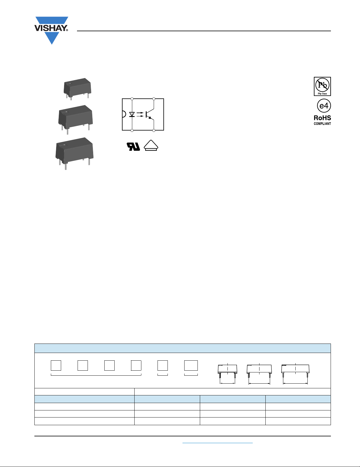
17187-4
CNY65
CNY66
CNY64
CNY64, CNY65, CNY66
Vishay Semiconductors
Optocoupler, Phototransistor Output, Very High Isolation Voltage
FEATURES
Top View
A
C
17187-5
V
DE
C
E
DESCRIPTION
The CNY64, CNY65, and CNY66 consist of a
phototransistor optically coupled to a gallium arsenide
infrared-emitting diode in a 4 pin plastic package.
The single components are mounted opposite one another,
providing a distance between input and output for highest
safety requirements of > 3 mm.
VDE STANDARDS
These couplers perform safety functions according to the
following equipment standards:
• DIN EN 60747-5-2 (VDE 0884)
Optocoupler for electrical safety requirements
• IEC 60950/EN 60950
Office machines
• VDE 0804
Telecommunication apparatus and data processing
• IEC60065
Safety for mains-operated electronic and related
household apparatus
• VDE 0700/IEC 60335
Household equipment
• VDE 0160
Electronic equipment for electrical power installation
• VDE 0750/IEC60601
Medical equipment
• Rated recurring peak voltage (repetitive)
V
= 1450 V
IORM
peak
• Thickness through insulation 3 mm
• Creepage current resistance according to
VDE 0303/IEC 60112 comparative tracking
index: CTI 200
• Compliant to RoHS Directive 2002/95/EC and in
accordance to WEEE 2002/96/EC
APPLICATIONS
Circuits for safe protective separation against electrical
shock according to safety class II (reinforced isolation):
• for appl. class I - IV at mains voltage 300 V
• for appl. class I - IV at mains voltage 600 V
• for appl. class I - III at mains voltage 1000 V according
to DIN EN 60747-5-2 (VDE 0884), suitable for:
- Switch-mode power supplies
- Line receiver
- Computer peripheral interface
- Microprocessor system interface
AGENCY APPROVALS
• UL1577, file no. E76222 system code H, J, and K
• DIN EN 60747-5-2 (VDE 0884)/DIN EN 60747-5-5
(pending), available with option 1
• VDE related features:
- rated impulse voltage (transient overvoltage),
V
= 12 kV peak
IOTM
- isolation test voltage (partial discharge test voltage),
= 2.8 kV peak
V
pd
ORDERING INFORMATION
DIP, 400 mil DIP, 600 mil DIP, 700 mil
CNY 6 # x
PART NUMBER PACKAGE
AGENCY CERTIFIED/PACKAGE CTR (%)
UL, VDE 50 to 300 63 to 125 100 to 200
DIP-4 HV, 400 mil, high isolation distance CNY64 CNY64A CNY64B
DIP-4 HV, 600 mil, high isolation distance CNY65 CNY65A CNY65B
DIP-4 HV, 700 mil, high isolation distance CNY66 - CNY66B
Document Number: 83540 For technical questions, contact: optocoupleranswers@vishay.com
Rev. 2.1, 24-Feb-11 1
OPTION
CTR
BIN
10.16 mm
15.24 mm
17.8 mm
www.vishay.com
Page 2
CNY64, CNY65, CNY66
Vishay Semiconductors
Optocoupler, Phototransistor Output,
Very High Isolation Voltage
ABSOLUTE MAXIMUM RATINGS (T
PARAMETER TEST CONDITION SYMBOL VALUE UNIT
INPUT
Reverse voltage V
Forward current I
Forward surge current t
Power dissipation P
Junction temperature T
OUTPUT
Collector emitter voltage V
Emitter collector voltage V
Collector current I
Collector peak current t
Power dissipation P
Junction temperature T
COUPLER
AC isolation test voltage CNY64 t = 1 min V
DC isolation test voltage CNY65 t = 1 s V
DC isolation test voltage CNY66 t = 1 s V
Total power dissipation P
Ambient temperature range T
Storage temperature range T
Soldering temperature 2 mm from case, 10 s T
Note
• Stresses in excess of the absolute maximum ratings can cause permanent damage to the device. Functional operation of the device is not
implied at these or any other conditions in excess of those given in the operational sections of this document. Exposure to absolute
maximum ratings for extended periods of the time can adversely affect reliability.
= 25 °C, unless otherwise specified)
amb
10 μs I
p
/T = 0.5, tp 10 ms I
p
FSM
diss
CEO
ECO
CM
diss
ISO
ISO
ISO
amb
stg
sld
R
F
5V
75 mA
1.5 A
120 mW
j
100 °C
32 V
7V
C
50 mA
100 mA
130 mW
j
100 °C
8200 V
RMS
13.9 kV
13.9 kV
tot
250 mW
- 55 to + 85 °C
- 55 to + 100 °C
260 °C
ELECTRICAL CHARACTERISTICS (T
= 25 °C, unless otherwise specified)
amb
PARAMETER TEST CONDITION SYMBOL MIN. TYP. MAX. UNIT
INPUT
Forward voltage I
Junction capacitance V
= 50 mA V
F
= 0, f = 1 MHz C
R
F
j
1.25 1.6 V
50 pF
OUTPUT
Collector emitter voltage I
Emitter collector voltage I
Collector emitter leakage current V
= 1 mA V
C
= 100 μA V
E
= 20 V, IF = 0 A I
CE
CEO
ECO
CEO
32 V
7V
200 nA
COUPLER
Collector emitter saturation voltage I
Cut-off frequency
Coupling capacitance f = 1 MHz C
= 10 mA, IC = 1 mA V
F
V
= 5 V, IF = 10 mA,
CE
R
= 100
L
CEsat
f
c
k
0.3 V
110 kHz
0.3 pF
Note
• Minimum and maximum values are testing requirements. Typical values are characteristics of the device and are the result of engineering
evaluation. Typical values are for information only and are not part of the testing requirements.
www.vishay.com For technical questions, contact: optocoupleranswers@vishay.com
Document Number: 83540
2 Rev. 2.1, 24-Feb-11
Page 3
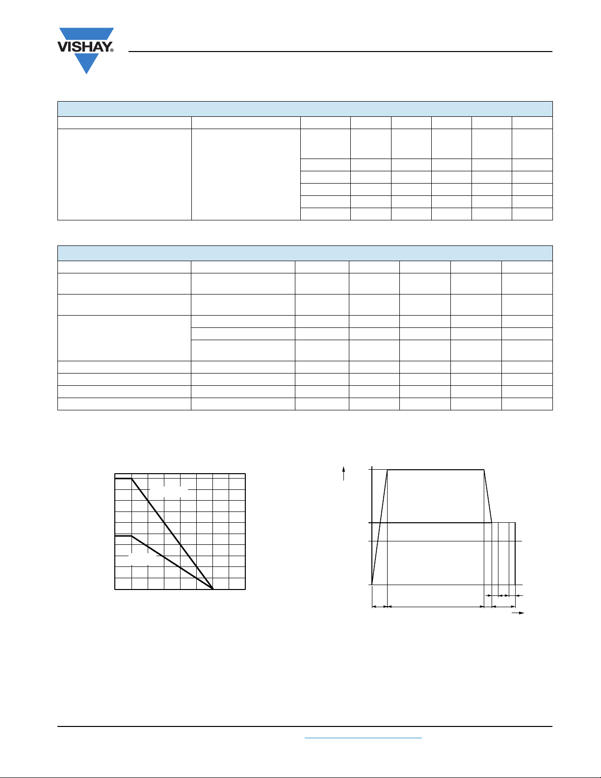
0
25
50
75
100
125
150
175
200
225
250
0 25 50 75 100 125 150 175 200
TSI - Safety Temperature(°C)
P
SO
(mW)
ISI(mA)
t
13930
t1, t2 = 1 to 10 s
t
3
, t4 = 1 s
t
test
= 10 s
t
stres
= 12 s
V
IOTM
V
Pd
V
IOWM
V
IORM
0
t
1
t
test
tTr = 60 s
t
stres
t3t
4
t
2
CNY64, CNY65, CNY66
Optocoupler, Phototransistor Output,
Vishay Semiconductors
Very High Isolation Voltage
CURRENT TRANSFER RATIO (T
PARAMETER TEST CONDITION PART SYMBOL MIN. TYP. MAX. UNIT
I
C/IF
SAFETY AND INSULATION RATED PARAMETERS
PARAMETER TEST CONDITION SYMBOL MIN. TYP. MAX. UNIT
Partial discharge test voltage routine test
Partial discharge test voltage lot test (sample test)
V
IO
V
Insulation resistance
Forward current I
Power dissipation P
Rated impulse voltage V
Safety temperature T
Note
• According to DIN EN 60747-5-2 (see fig. 2). This optocoupler is suitable for safe electrical isolation only within the safety ratings. Compliance
with the safety ratings shall be ensured by means of suitable protective circuits.
IO
V
IO
(construction test only)
= 25 °C, unless otherwise specified)
amb
CNY64,
CNY65,
CNY66
CNY64A CTR 63 125 %
VCE = 5 V, IF = 10 mA
CNY65A CTR 63 125 %
CNY64B CTR 100 200 %
CNY65B CTR 100 200 %
CNY66B CTR 100 200 %
100 %, t
t
= 60 s, t
Tr
= 500 V, T
= 500 V, T
= 500 V, T
= 1 s V
test
= 10 s,
test
(see fig. 2)
amb
= 100 °C R
amb
= 150 °C
amb
= 25 °C R
pd
V
pd
IO
IO
R
IO
SI
SO
IOTM
SI
CTR 50 300 %
2.8 kV
2.2 kV
12
10
10
10
11
9
120 mA
250 mW
12 kV
150 °C
Document Number: 83540 For technical questions, contact: optocoupleranswers@vishay.com
Rev. 2.1, 24-Feb-11 3
Fig. 1 - Safety Derating Diagram Fig. 2 - Test Pulse Diagram for Sample Test According to
DIN EN 60747-5-2 (VDE 0884); IEC60747-5-5
www.vishay.com
Page 4

CNY64, CNY65, CNY66
Channel I
Channel II
95 10900
RG = 50
t
p
tp = 50 µs
T
= 0.01
+ 5 V
I
C
= 5 mA; adjusted through
input amplitude
I
F
0
I
F
50 100
Oscilloscope
R
L
1 M
C
L
20 pF
Channel I
Channel II
95 10843
RG= 50 Ω
t
p
tp= 50 µs
T
= 0.01
+ 5 V
I
C
I
F
0
50 Ω
1 kΩ
I
F
= 10 mA
Oscilloscope
R
L
≥
C
L
20 pF
1 MΩ
≤
Vishay Semiconductors
Optocoupler, Phototransistor Output,
Very High Isolation Voltage
SWITCHING CHARACTERISTICS (T
PARAMETER TEST CONDITION SYMBOL MIN. TYP. MAX. UNIT
Delay time V
Rise time V
Fall time V
Storage time V
Turn-on time V
Turn-off time V
Turn-on time V
Turn-off time V
Fig. 3 - Test Circuit, Non-Saturated Operation
= 5 V, IC = 5 mA, RL = 100 , (see fig. 3) t
S
= 5 V, IC = 5 mA, RL = 100 , (see fig. 3) t
S
= 5 V, IC = 5 mA, RL = 100 , (see fig. 3) t
S
= 5 V, IC = 5 mA, RL = 100 , (see fig. 3) t
S
= 5 V, IC = 5 mA, RL = 100 , (see fig. 3) t
S
= 5 V, IC = 5 mA, RL = 100 , (see fig. 3) t
S
= 5 V, IF = 10 mA, RL = 1 k, (see fig. 4) t
S
= 5 V, IF = 10 mA, RL = 1 k, (see fig. 4) t
S
= 25 °C, unless otherwise specified)
amb
d
r
f
s
on
off
on
off
I
F
0
I
C
100 %
90 %
10 %
0
t
p
t
d
t
r
t
(= td + tr) Turn-on time
on
2.6 μs
2.4 μs
2.7 μs
0.3 μs
5μs
3μs
25 μs
42.5 μs
t
p
t
r
t
d
t
on
Pulse duration
Delay time
Rise time
t
s
t
s
t
f
(= ts + tf) Turn-off time
t
off
Fig. 5 - Switching Times
t
t
f
t
off
t
Storage time
Fall time
96 11698
Fig. 4 - Test Circuit, Saturated Operation
www.vishay.com For technical questions, contact: optocoupleranswers@vishay.com
4 Rev. 2.1, 24-Feb-11
Document Number: 83540
Page 5

0.1
1
10
100
1000
0
VF - Forward Voltage (V)
96 11862
I
F
- Forward Current (mA)
1.6
1.2
0.8
0.4
2.0
0.5
0.6
0.7
0.8
0.9
1.0
1.1
1.2
1.3
1.4
1.5
- 30 - 20 - 10 0
10 20 30 40 50 60 70 80
T
amb
- Ambient Temperature (°C)
96 11911
CTR
rel
- Relative Current Transfer Ratio
V
CE
= 5 V
I
F
= 10 mA
1
10
100
1000
0 102030405060708090 100
T
amb
- Ambient Temperature (°C)
96 12000
I
CEO
- Collector Dark Current,
with open Base (nA)
VCE = 20 V
I
F
= 0
CNY64, CNY65, CNY66
Optocoupler, Phototransistor Output,
Very High Isolation Voltage
TYPICAL CHARACTERISTICS (T
280
Coupled device
240
200
160
Phototransistor
120
IR-diode
80
40
- Total Power Dissipation (mW)
tot
0
P
0255075
T
21995
Fig. 6 - Total Power Dissipation vs. Ambient Temperature
- Ambient Temperature (°C)
amb
= 25 °C, unless otherwise specified)
amb
Vishay Semiconductors
100
Fig. 9 - Collector Dark Current vs. Ambient Temperature
100
VCE = 5 V
10
Fig. 7 - Forward Current vs. Forward Voltage
Fig. 8 - Relative Current Transfer Ratio vs.
Document Number: 83540 For technical questions, contact: optocoupleranswers@vishay.com
Rev. 2.1, 24-Feb-11 5
Ambient Temperature
1
0.1
- Collector Current (mA)
C
I
0.01
0.1 1 10
95 11012
IF - Forward Current (mA)
100
Fig. 10 - Collector Current vs. Forward Current
100
10
1
- Collector Current (mA)
C
I
0.1
0.1 1 10
95 11013
VCE - Collector Emitter Voltage (V)
IF = 50 mA
10 mA
5 mA
2 mA
1 mA
100
Fig. 11 - Collector Current vs. Collector Emitter Voltage
www.vishay.com
Page 6

CNY64, CNY65, CNY66
0.0
0.1
0.2
0.3
0.4
0.5
0.6
0.7
0.8
0.9
1.0
110100
IC - Collector Current (mA)
96 11912
V
CEsat
- Collector Emitter
Saturation Voltage (V)
CTR = 50 %
10 %
20 %
01015
0
10
20
30
40
50
IF - Forward Current (mA)
20
95 11017
t
on
/t
off
- Turn-on/Turn-off Time (µs)
Saturated operation
V
S
= 5 V
R
L
= 1 kΩ
t
off
t
on
5
04
IC - Collector Current (mA)
10
95 11016
Non-saturated
operation
V
S
= 5 V
R
L
= 100 Ω
t
off
t
on
0
5
10
15
20
8
t
on
/t
off
- Turn-on/Turn-off Time (µs)
2
6
Vishay Semiconductors
Fig. 12 - Collector Emitter Saturation Voltage vs.
Collector Current
1000
Optocoupler, Phototransistor Output,
Very High Isolation Voltage
Fig. 15 - Turn-on/Turn-off Time vs. Forward Current
VCE = 5 V
100
10
CTR - Current Transfer Ratio (%)
1
0.1 1 10
95 11015
IF - Forward Current (mA)
Fig. 13 - Current Transfer Ratio vs. Forward Current
Fig. 14 - Turn-on/Turn-off Time vs. Collector Current
www.vishay.com For technical questions, contact: optocoupleranswers@vishay.com
6 Rev. 2.1, 24-Feb-11
100
Document Number: 83540
Page 7

CNY64, CNY65, CNY66
Optocoupler, Phototransistor Output,
Very High Isolation Voltage
PACKAGE DIMENSIONS in millimeters FOR CNY64
12.8 ± 0.1
6.01 ± 0.1
10.16 ± 0.2
0.4
A
0.5
Coll
Vishay Semiconductors
7.2 ± 0.1
9.1 ± 0.3
5.08 ± 0.2
Weight: ca. 0.73 g
Creepage distance: > 9.5 mm
Air path: > 9.5 mm
after mounting on PC board
Cath
Drawing-No.: 6.544-5038.01-4
Issue: 2; 10.11.98
14765
E
technical drawings
according to DIN
specifications
Document Number: 83540 For technical questions, contact: optocoupleranswers@vishay.com
www.vishay.com
Rev. 2.1, 24-Feb-11 7
Page 8
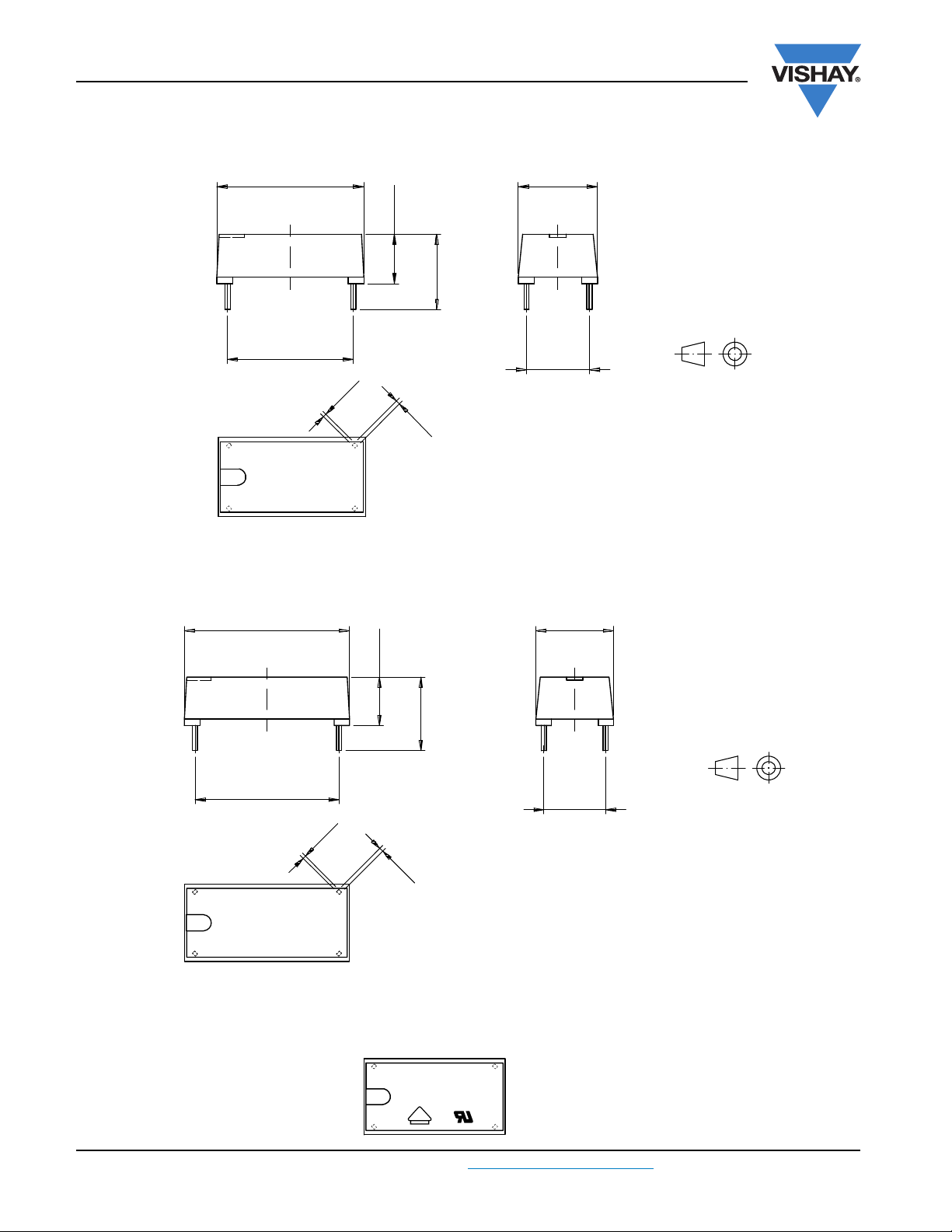
CNY64, CNY65, CNY66
14764
technical drawings
according to DIN
specifications
Weight: ca. 1.70 g
Creepage distance: > 17 mm
Air path: > 17 mm
after mounting on PC board
9.6 ± 0.1
20.4 ± 0.1
17.8 ± 0.2
7.62 ± 0.2
Cath
A
Coll
E
0.4
0.5
6.1 ± 0.1
9.1 ± 0.3
Drawing-No.: 6.544-5037.01-4
Issue: x; 10.11.98
Vishay Semiconductors
Optocoupler, Phototransistor Output,
Very High Isolation Voltage
PACKAGE DIMENSIONS in millimeters FOR CNY65
17.8 ± 0.1
6.1 ± 0.1
9.1 ± 0.3
15.24 ± 0.2
0.4
0.5
A
Cath
Drawing-No.: 6.544-5036.01-1
Issue: 2; 10.11.98
14763
Coll
E
9.6 ± 0.1
7.62 ± 0.2
Weight: ca. 1.40 g
Creepage distance: > 14 mm
Air path: > 14 mm
after mounting on PC board
technical drawings
according to DIN
specifications
PACKAGE DIMENSIONS in millimeters FOR CNY66
PACKAGE MARKING
www.vishay.com For technical questions, contact: optocoupleranswers@vishay.com
8 Rev. 2.1, 24-Feb-11
21764-73
CNY65A
V YWW J 69
Document Number: 83540
Page 9

Legal Disclaimer Notice
www.vishay.com
Vishay
Disclaimer
ALL PRODUCT, PRODUCT SPECIFICATIONS AND DATA ARE SUBJECT TO CHANGE WITHOUT NOTICE TO IMPROVE
RELIABILITY, FUNCTION OR DESIGN OR OTHERWISE.
Vishay Intertechnology, Inc., its affiliates, agents, and employees, and all persons acting on its or their behalf (collectively,
“Vishay”), disclaim any and all liability for any errors, inaccuracies or incompleteness contained in any datasheet or in any other
disclosure relating to any product.
Vishay makes no warranty, representation or guarantee regarding the suitability of the products for any particular purpose or
the continuing production of any product. To the maximum extent permitted by applicable law, Vishay disclaims (i) any and all
liability arising out of the application or use of any product, (ii) any and all liability, including without limitation special,
consequential or incidental damages, and (iii) any and all implied warranties, including warranties of fitness for particular
purpose, non-infringement and merchantability.
Statements regarding the suitability of products for certain types of applications are based on Vishay’s knowledge of
typical requirements that are often placed on Vishay products in generic applications. Such statements are not binding
statements about the suitability of products for a particular application. It is the customer’s responsibility to validate that a
particular product with the properties described in the product specification is suitable for use in a particular application.
Parameters provided in datasheets and / or specifications may vary in different applications and performance may vary over
time. All operating parameters, including typical parameters, must be validated for each customer application by the customer’s
technical experts. Product specifications do not expand or otherwise modify Vishay’s terms and conditions of purchase,
including but not limited to the warranty expressed therein.
Except as expressly indicated in writing, Vishay products are not designed for use in medical, life-saving, or life-sustaining
applications or for any other application in which the failure of the Vishay product could result in personal injury or death.
Customers using or selling Vishay products not expressly indicated for use in such applications do so at their own risk.
Please contact authorized Vishay personnel to obtain written terms and conditions regarding products designed for
such applications.
No license, express or implied, by estoppel or otherwise, to any intellectual property rights is granted by this document
or by any conduct of Vishay. Product names and markings noted herein may be trademarks of their respective owners.
© 2019 VISHAY INTERTECHNOLOGY, INC. ALL RIGHTS RESERVED
Revision: 01-Jan-2019
1
Document Number: 91000
 Loading...