

Page 1
www.vishay.com
1
2
3
6
5
4
NC
C
E
A
C
NC
i179004-14
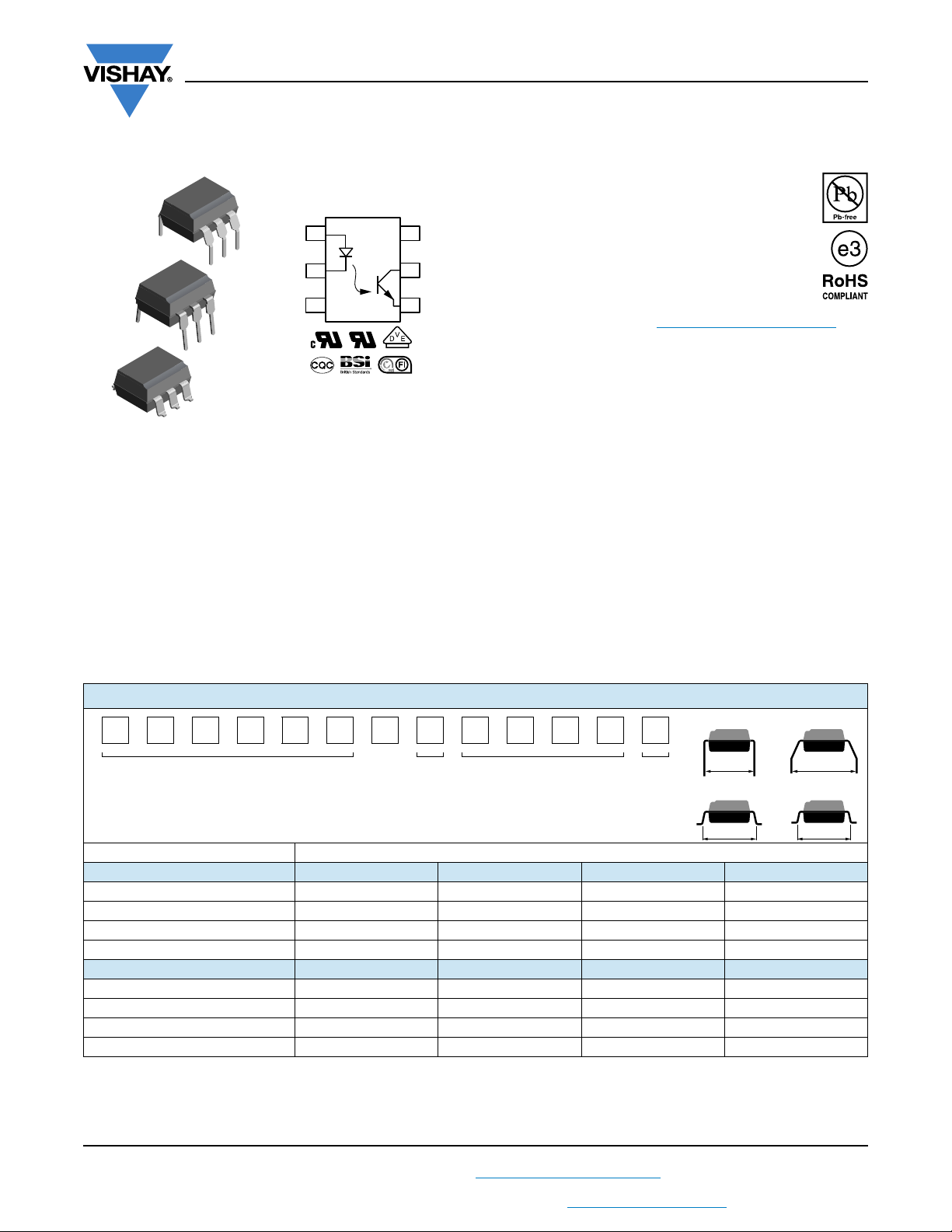
Optocoupler, Phototransistor Output, no Base Connection
DESCRIPTION
The CNY17F is an optocoupler consisting of a gallium
arsenide infrared emitting diode optically coupled to a
silicon planar phototransistor detector in a plastic plug-in
DIP-6 package.
The coupling device is suitable for signal transmission
between two electrically separated circuits. The potential
difference between the circuits to be coupled is not allowed
to exceed the maximum permissible reference voltages.
In contrast to the CNY17 series, the base terminal of the
F type is not conected, resulting in a substantially improved
common-mode interference immunity.
CNY17F
Vishay Semiconductors
FEATURES
• Isolation test voltage, 5000 V
• No base terminal connection for improved
common mode interface immunity
• Long term stability
• Industry standard dual-in-line package
• Material categorization: For definitions of
compliance please see www.vishay.com/doc?99912
AGENCY APPROVALS
Safety application model number covering all products in
this datasheet is CNY17F. This model number should be
used when consulting safety agency documents.
• UL file no. E52744
• cUL tested to CSA 22.2 bulletin 5A
• DIN EN 60747-5-5 (VDE 0884-5), available with option 1
• BSI: EN 60065, EN 60950-1
• FIMKO EN60950
• CQC GB8898-2011
RMS
ORDERING INFORMATION
CNY17F - #X0 ##T
DIP-6
PART NUMBER CTR
BIN
PACKAGE OPTION TAPE
AND
REEL
7.62 mm 10.16 mm
Option 7
> 8 mm
AGENCY CERTIFIED/PACKAGE CTR (%)
UL, cUL, BSI, FIMKO 40 to 80 63 to 125 100 to 200 160 to 320
DIP-6 CNY17F-1 CNY17F-2 CNY17F-3 CNY17F-4
DIP-6, 400 mil, option 6 CNY17F-1X006 CNY17F-2X006 CNY17F-3X006 CNY17F-4X006
SMD-6, option 7 CNY17F-1X007
SMD-6, option 9 CNY17F-1X009T
(1)
(1)
CNY17F-2X007T
CNY17F-2X009T
(1)
(1)
CNY17F-3X007T
CNY17F-3X009T
(1)
(1)
CNY17F-4X007T
CNY17F-4X009T
VDE, UL, cUL, BSI, FIMKO 40 to 80 63 to 125 100 to 200 160 to 320
DIP-6 CNY17F-1X001 CNY17F-2X001 CNY17F-3X001 CNY17F-4X001
DIP-6, 400 mil, option 6 CNY17F-1X016 CNY17F-2X016 CNY17F-3X016 CNY17F-4X016
SMD-6, option 7 CNY17F-1X017
(1)
CNY17F-2X017
SMD-6, option 9 CNY17F-1X019 CNY17F-2X019
(1)
(1)
CNY17F-3X017
CNY17F-3X019
(1)
(1)
CNY17F-4X017
Notes
• Additional options may be possible, please contact sales office.
(1)
Rev. 2.2, 08-Jan-14
Also available in tubes; do not put T on end.
THIS DOCUMENT IS SUBJECT TO CHANGE WITHOUT NOTICE. THE PRODUCTS DESCRIBED HEREIN AND THIS DOCUMENT
ARE SUBJECT TO SPECIFIC DISCLAIMERS, SET FORTH AT www.vishay.com/doc?91000
For technical questions, contact: optocoupleranswers@vishay.com
1
Document Number: 83607
Option 6
Option 9
8 mm typ.
(1)
(1)
(1)
-
Page 2
www.vishay.com
CNY17F
Vishay Semiconductors
ABSOLUTE MAXIMUM RATINGS (T
= 25 °C, unless otherwise specified)
amb
PARAMETER TEST CONDITION SYMBOL VALUE UNIT
INPUT
Reverse voltage V
DC forward current I
Surge forward current t ≤ 10 μs I
Power dissipation P
R
F
FSM
diss
6V
60 mA
2.5 A
100 mW
OUTPUT
Collector emitter breakdown voltage BV
Collector current I
Collector peak current t
/T = 0.5, tp ≤ 10 ms I
p
Output power dissipation P
CEO
C
CM
diss
70 V
50 mA
100 mA
150 mW
COUPLER
Isolation test voltage between emitter and
detector
Storage temperature range T
Ambient temperature range T
Junction temperature T
Soldering temperature
(1)
Total power dissipation P
t = 1 min V
2 mm from case, ≤ 10 s T
ISO
stg
amb
sld
diss
5000 V
RMS
-55 to +150 °C
-55 to +110 °C
j
100 °C
260 °C
250 mW
Notes
• Stresses in excess of the absolute maximum ratings can cause permanent damage to the device. Functional operation of the device is not
implied at these or any other conditions in excess of those given in the operational sections of this document. Exposure to absolute
maximum ratings for extended periods of the time can adversely affect reliability.
(1)
Refer to reflow profile for soldering conditions for surface mounted parts (SMD). Refer to wave profile for soldering conditions for through
hole parts (DIP).
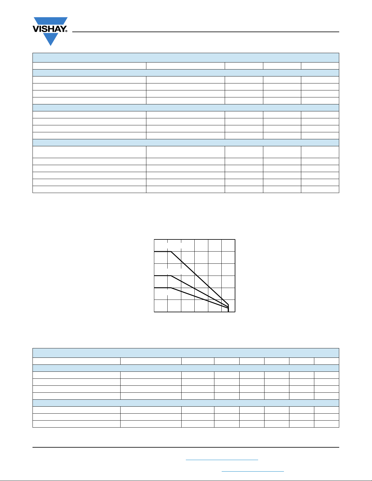
300
250
200
150
100
- Total Power Dissipation (mW)
tot
P
Coupled device
Phototransistor
IR-diode
50
0
0 20 40 60 80 100 120
T
- Ambient Temperature (°C)
amb
Fig. 1 - Total Power Dissipation vs. Ambient Temperature
ELECTRICAL CHARACTERISTICS (T
= 25 °C, unless otherwise specified)
amb
PARAMETER TEST CONDITION PART SYMBOL MIN. TYP. MAX. UNIT
INPUT
Forward voltage I
Breakdown voltage I
Reverse current V
Capacitance V
= 60 mA V
F
= 10 μA V
R
= 6 V I
R
= 0 V, f = 1 MHz C
R
BR
R
F
1.39 1.65 V
6V
0.01 10 μA
O
25 pF
OUTPUT
Collector emitter capacitance V
Base collector capacitance V
Emitter base capacitance V
= 5 V, f = 1 MHz C
CE
= 5 V, f = 1 MHz C
CE
= 5 V, f = 1 MHz C
CE
CE
BC
EB
5.2 pF
6.5 pF
7.5 pF
Rev. 2.2, 08-Jan-14
2
Document Number: 83607
For technical questions, contact: optocoupleranswers@vishay.com
THIS DOCUMENT IS SUBJECT TO CHANGE WITHOUT NOTICE. THE PRODUCTS DESCRIBED HEREIN AND THIS DOCUMENT
ARE SUBJECT TO SPECIFIC DISCLAIMERS, SET FORTH AT www.vishay.com/doc?91000
Page 3
www.vishay.com
CNY17F
Vishay Semiconductors
ELECTRICAL CHARACTERISTICS (T
= 25 °C, unless otherwise specified)
amb
PARAMETER TEST CONDITION PART SYMBOL MIN. TYP. MAX. UNIT
COUPLER
Collector emitter, saturation voltage I
= 10 mA, IC = 2.5 mA V
F
Coupling capacitance C
CNY17F-1 I
Collector emitter, leakage current V
= 10 V
CE
CNY17F-2 I
CNY17F-3 I
CNY17F-4 I
CEsat
C
CEO
CEO
CEO
CEO
0.25 0.4 V
0.6 pF
250nA
250nA
5 100 nA
5 100 nA
Note
• Minimum and maximum values were tested requierements. Typical values are characteristics of the device and are the result of engineering
evaluations. Typical values are for information only and are not part of the testing requirements.
CURRENT TRANSFER RATIO (T
= 25 °C, unless otherwise specified)
amb
PARAMETER TEST CONDITION PART SYMBOL MIN. TYP. MAX. UNIT
CNY17F-1 CTR 40 80 %
CNY17F-2 CTR 63 125 %
CNY17F-3 CTR 100 200 %
CNY17F-4 CTR 160 320 %
CNY17F-1 CTR 13 30 %
CNY17F-2 CTR 22 45 %
CNY17F-3 CTR 34 70 %
I
C/IF
IF = 10 mA
I
= 1 mA
F
CNY17F-4 CTR 56 90 %
Note
• Current transfer ratio I
at VCE = 5 V, 25 °C and collector emitter leakage current by dash number.
C/IF
SWITCHING CHARACTERISTICS (T
= 25 °C, unless otherwise specified)
amb
PARAMETER TEST CONDITION PART SYMBOL MIN. TYP. MAX. UNIT
LINEAR OPERATION (without saturation)
= 10 mA, VCC = 5 V,
I
Turn-on time
Rise time
Turn-off time
Fall time
Cut-off frequency
F
R
= 75 Ω
L
I
= 10 mA, VCC = 5 V,
F
R
= 75 Ω
L
I
= 10 mA, VCC = 5 V,
F
R
= 75 Ω
L
IF = 10 mA, VCC = 5 V,
R
= 75 Ω
L
I
= 10 mA, VCC = 5 V,
F
R
= 75 Ω
L
t
on
t
r
t
off
t
f
f
CO
3μs
2μs
2.3 μs
2μs
110 kHz
SWITCHING OPERATION (with saturation)
Turn-on time
Rise time
Turn-off time
Fall time
Rev. 2.2, 08-Jan-14
= 20 mA CNY17F-1 t
I
F
I
= 10 mA
F
I
= 5 mA CNY17F-4 t
F
= 20 mA CNY17F-1 t
I
F
I
= 10 mA
F
= 5 mA CNY17F-4 t
I
F
I
= 20 mA CNY17F-1 t
F
= 10 mA
I
F
I
= 5 mA CNY17F-4 t
F
I
= 20 mA CNY17F-1 t
F
= 10 mA
I
F
I
= 5 mA CNY17F-4 t
F
CNY17F-2 t
CNY17F-3 t
CNY17F-2 t
CNY17F-3 t
CNY17F-2 t
CNY17F-3 t
CNY17F-2 t
CNY17F-3 t
3
on
on
on
on
r
r
r
r
off
off
off
off
f
f
f
f
3μs
4.2 μs
4.2 μs
6μs
2μs
3μs
3μs
4.6 μs
18 μs
23 μs
23 μs
25 μs
11 μs
14 μs
14 μs
15 μs
Document Number: 83607
For technical questions, contact: optocoupleranswers@vishay.com
THIS DOCUMENT IS SUBJECT TO CHANGE WITHOUT NOTICE. THE PRODUCTS DESCRIBED HEREIN AND THIS DOCUMENT
ARE SUBJECT TO SPECIFIC DISCLAIMERS, SET FORTH AT www.vishay.com/doc?91000
Page 4

www.vishay.com
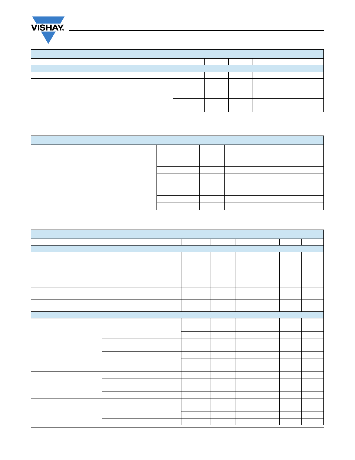
Channel I
Channel II
95 10804-3
RG = 50 Ω
t
p
tp = 50 µs
T
= 0.01
+ 5 V
I
F
0
50 Ω R
L
I
F
Oscilloscope
R
L
= 1 MΩ
C
L
= 20 pF
Channel I
Channel II
95 10843
RG= 50 Ω
t
p
tp= 50 µs
T
= 0.01
+ 5 V
I
C
I
F
0
50 Ω
1 kΩ
I
F
= 10 mA
Oscilloscope
R
L
≥
C
L
20 pF
1 MΩ
≤
Fig. 2 - Test Circuit, Non-Saturated Operation
Fig. 3 - Test Circuit, Saturated Operation
CNY17F
Vishay Semiconductors
I
F
0
I
C
100 %
90 %
10 %
0
t
p
t
d
t
r
(= td + tr) Turn-on time
t
on
t
t
p
t
r
d
t
on
Pulse duration
Delay time
Rise time
t
t
s
t
f
t
off
Fig. 4 - Switching Times
t
t
f
s
t
off
(= ts + tf) Turn-off time
t
Storage time
Fall time
96 11698
SAFETY AND INSULATION RATINGS
PARAMETER SYMBOL VALUE UNIT
MAXIMUM SAFETY RATINGS
Output safety power P
Input safety current I
Safety temperature T
SO
SI
SI
Comparative tracking index CTI 175
INSULATION RATED PARAMETERS
Maximum withstanding isolation voltage V
Maximum transient isolation voltage V
Maximum repetitive peak isolation voltage V
Insulation resistance T
Isolation resistance T
= 25 °C, VDC = 500 V R
amb
= 100 °C, VDC = 500 V R
amb
ISO
IOTM
IORM
IO
IO
Climatic classification (according to IEC 68 part 1) 55/115/21
Environment (pollution degree in accordance to DIN VDE 0109) 2
Creepage distance
Clearance distance
Insulation thickness DTI ≥ 0.4 mm
Note
• As per DIN EN 60747-5-5, § 7.4.3.8.2, this optocoupler is suitable for “safe electrical insulation” only within the safety ratings. Compliance
with the safety ratings shall be ensured by means of protective circuits.
Rev. 2.2, 08-Jan-14
THIS DOCUMENT IS SUBJECT TO CHANGE WITHOUT NOTICE. THE PRODUCTS DESCRIBED HEREIN AND THIS DOCUMENT
ARE SUBJECT TO SPECIFIC DISCLAIMERS, SET FORTH AT www.vishay.com/doc?91000
Standard DIP-4 ≥ 7mm
SMD ≥ 7mm
Standard DIP-4 ≥ 8mm
SMD ≥ 8mm
For technical questions, contact: optocoupleranswers@vishay.com
4
700 mW
400 mA
175 °C
5000 V
8000 V
890 V
12
≥ 10
11
≥ 10
Document Number: 83607
RMS
peak
peak
Ω
Ω
Page 5

www.vishay.com
0.6
0.8
0.9
1.0
1.1
1.2
1.3
1.4
1.8
0.1 1 10 100
I
F
- Forward Current (mA)
V
F
- Forward Voltage (V)
T
amb
= - 55 °C
1.5
0.7
T
amb
= - 40 °C
T
amb
= 100 °C
T
amb
= 75 °C
T
amb
= 50 °C
T
amb
= 25 °C
T
amb
= 0 °C
T
amb
= - 25 °C
1.6
1.7
T
amb
= 110 °C
0
20
30
40
50
60
01 78
V
CE
- Collector Emitter Voltage (NS) (V)
I
C
- Collector Current (mA)
10
65432
IF = 20 mA
IF = 15 mA
IF = 10 mA
IF = 30 mA
IF = 5 mA
0
10
15
20
25
00.4
V
CE
- Collector Emitter Voltage (sat) (V)
I
C
- Collector Current (mA)
5
0.30.20.1
IF = 10 mA
IF = 25 mA
IF = 5 mA
IF = 2 mA
IF = 1 mA
0.001
0.01
0.1
10
1
100
1000
10 000
- 60 100
T
amb
- Ambient Temperature (°C)
I
CE0
- Leakage Current (nA)
VCE = 40 V
- 40 806040200- 20
IF = 0 mA
VCE = 12 V
VCE = 24 V
0
0.2
0.6
0.4
0.8
1.0
1.2
-60 120
T
amb
- Ambient Temperature (°C)
CTR
Norm
- Normalized CTR (NS)
-40 806040200-20
IF = 10 mA
VCE = 5 V
100
0
0.2
0.6
0.4
0.8
1.0
1.2
-60 120
T
amb
- Ambient Temperature (°C)
CTR
Norm
- Normalized CTR (sat)
-40 806040200-20
IF = 10 mA
VCE = 0.4 V
100
CNY17F
Vishay Semiconductors
TYPICAL CHARACTERISTICS (T
Fig. 5 - Forward Voltage vs. Forward Current
= 25 °C, unless otherwise specified)
amb
Fig. 8 - Leakage Current vs. Ambient Temperature
Fig. 6 - Collector Current vs. Collector Emitter Voltage (NS)
Rev. 2.2, 08-Jan-14
Fig. 7 - Collector Current vs. Collector Emitter Voltage (sat)
THIS DOCUMENT IS SUBJECT TO CHANGE WITHOUT NOTICE. THE PRODUCTS DESCRIBED HEREIN AND THIS DOCUMENT
ARE SUBJECT TO SPECIFIC DISCLAIMERS, SET FORTH AT www.vishay.com/doc?91000
For technical questions, contact: optocoupleranswers@vishay.com
Fig. 9 - Normalized CTR (NS) vs. Ambient Temperature
Fig. 10 - Normalized CTR (sat) vs. Ambient Temperature
5
Document Number: 83607
Page 6

www.vishay.com
0
0.2
0.6
0.4
0.8
1.0
1.2
0.1 100
I
F
- Forward Current (mA)
CTR
Norm
- Normalized CTR (NS)
110
T
amb
= - 55 °C
T
amb
= - 40 °C
T
amb
= 0 °C
T
amb
= 25 °C
T
amb
= 50 °C
T
amb
= 75 °C
T
amb
= 110 °C
VCE = 5 V
T
amb
= 100 °C
IF = 10 mA
0
0.2
0.6
0.4
0.8
1.0
1.2
0.1 100
I
F
- Forward Current (mA)
CTR
Norm
- Normalized CTR (sat)
110
T
amb
= - 55 °C
T
amb
= - 40 °C
T
amb
= 0 °C
T
amb
= 25 °C
T
amb
= 50 °C
T
amb
= 75 °C
T
amb
= 110 °C
VCE = 0.4 V
T
amb
= 100 °C
IF = 10 mA
- 160
- 140
- 60
- 40
0
1 1000
f - Frequency (kHz)
Phase (deg)
- 20
10 100
VCE = 5 V
- 80
- 100
- 120
1
10
1000
0.1 100
I
C
- Collector Current (mA)
f
CTR
- CTR Frequency (kHz)
100
110
VCC = 5 V
0.1
1
10
1000
0.1 100
R
L
- Load Resistance (kΩ)
t
on
, t
off
- Switching Time (μs)
100
110
VCE = 5 V, IF = 10 mA
t
on
t
off
CNY17F
Vishay Semiconductors
Fig. 11 - Normalized CTR (NS) vs. Forward Current
Fig. 12 - Normalized CTR (sat) vs. Forward Current
Fig. 14 - CTR -3 dB Frequency vs. Collector Current
Fig. 15 - Switching Time vs. Load Resistance
Rev. 2.2, 08-Jan-14
THIS DOCUMENT IS SUBJECT TO CHANGE WITHOUT NOTICE. THE PRODUCTS DESCRIBED HEREIN AND THIS DOCUMENT
Fig. 13 - CTR Frequency vs. Phase Angle
6
For technical questions, contact: optocoupleranswers@vishay.com
ARE SUBJECT TO SPECIFIC DISCLAIMERS, SET FORTH AT www.vishay.com/doc?91000
Document Number: 83607
Page 7

www.vishay.com
20802-34
10.16 typ.
7.62 typ.
Option 6
8 min.
7.62 typ.
3.5 ± 0.3
0.6 min.
10.3 max.
0.35 ± 0.25
Option 7
Option 9
7.62 typ.
0.6 min.
0.1 ± 0.1
3.5 ± 0.3
3.5 ± 0.3
0.1 min.
2.7 min.
8.16 ± 0.8
10.16 ± 0.3
2.54
R 0.25
1.78
0.76
1.52
8 min.
11.05
2.54
R 0.25
1.78
0.76
1.52
8 min.
11.05
PACKAGE DIMENSIONS in millimeters
CNY17F
Vishay Semiconductors
654
6.5 ± 0.5
123
2.8 ± 0.5
22530
7.3 ± 0.5
1.1 ± 0.1
2.54 ± 0.25
3.5 ± 0.3
3.3 ± 0.5
0.5 ± 0.1
7.62 ± 0.3
0.5 typ.
0.26
7.62 to 9.98
PACKAGE MARKING (Example of CNY17F-2x017T)
CNY17F-2
Notes
Pin 1 I.D.
V YWW 25
• VDE logo is only marked on option 1 parts. Option information is not marked on the part.
• Tape and reel suffix (T) is not part of the package marking.
Rev. 2.2, 08-Jan-14
For technical questions, contact: optocoupleranswers@vishay.com
THIS DOCUMENT IS SUBJECT TO CHANGE WITHOUT NOTICE. THE PRODUCTS DESCRIBED HEREIN AND THIS DOCUMENT
ARE SUBJECT TO SPECIFIC DISCLAIMERS, SET FORTH AT www.vishay.com/doc?91000
7
Document Number: 83607
Page 8

22537-1
Ø 1.55 ± 0.05 1.75 ± 0.1
12 ± 0.1
0.3 ± 0.05
2 ± 0.1 4 ± 0.1
7.5 ± 0.1
16 ± 0.3
www.vishay.com
TUBE AND TAPE INFORMATION
DEVICES PER TUBE
TYPE UNITS/TUBE TUBES/BOX UNITS/BOX
DIP-6 50 40 2000
Vishay Semiconductors
CNY17F
Fig. 16 - Tape and Reel Drawing, 1000 Units per Reel
Rev. 2.2, 08-Jan-14
For technical questions, contact: optocoupleranswers@vishay.com
THIS DOCUMENT IS SUBJECT TO CHANGE WITHOUT NOTICE. THE PRODUCTS DESCRIBED HEREIN AND THIS DOCUMENT
ARE SUBJECT TO SPECIFIC DISCLAIMERS, SET FORTH AT www.vishay.com/doc?91000
8
Document Number: 83607
Page 9

Legal Disclaimer Notice
www.vishay.com
Vishay
Disclaimer
ALL PRODUCT, PRODUCT SPECIFICATIONS AND DATA ARE SUBJECT TO CHANGE WITHOUT NOTICE TO IMPROVE
RELIABILITY, FUNCTION OR DESIGN OR OTHERWISE.
Vishay Intertechnology, Inc., its affiliates, agents, and employees, and all persons acting on its or their behalf (collectively,
“Vishay”), disclaim any and all liability for any errors, inaccuracies or incompleteness contained in any datasheet or in any other
disclosure relating to any product.
Vishay makes no warranty, representation or guarantee regarding the suitability of the products for any particular purpose or
the continuing production of any product. To the maximum extent permitted by applicable law, Vishay disclaims (i) any and all
liability arising out of the application or use of any product, (ii) any and all liability, including without limitation special,
consequential or incidental damages, and (iii) any and all implied warranties, including warranties of fitness for particular
purpose, non-infringement and merchantability.
Statements regarding the suitability of products for certain types of applications are based on Vishay's knowledge of typical
requirements that are often placed on Vishay products in generic applications. Such statements are not binding statements
about the suitability of products for a particular application. It is the customer's responsibility to validate that a particular product
with the properties described in the product specification is suitable for use in a particular application. Parameters provided in
datasheets and / or specifications may vary in different applications and performance may vary over time. All operating
parameters, including typical parameters, must be validated for each customer application by the customer's technical experts.
Product specifications do not expand or otherwise modify Vishay's terms and conditions of purchase, including but not limited
to the warranty expressed therein.
Hyperlinks included in this datasheet may direct users to third-party websites. These links are provided as a convenience and
for informational purposes only. Inclusion of these hyperlinks does not constitute an endorsement or an approval by Vishay of
any of the products, services or opinions of the corporation, organization or individual associated with the third-party website.
Vishay disclaims any and all liability and bears no responsibility for the accuracy, legality or content of the third-party website
or for that of subsequent links.
Except as expressly indicated in writing, Vishay products are not designed for use in medical, life-saving, or life-sustaining
applications or for any other application in which the failure of the Vishay product could result in personal injury or death.
Customers using or selling Vishay products not expressly indicated for use in such applications do so at their own risk. Please
contact authorized Vishay personnel to obtain written terms and conditions regarding products designed for such applications.
No license, express or implied, by estoppel or otherwise, to any intellectual property rights is granted by this document or by
any conduct of Vishay. Product names and markings noted herein may be trademarks of their respective owners.
© 2022 VISHAY INTERTECHNOLOGY, INC. ALL RIGHTS RESERVED
Revision: 01-Jan-2022
1
Document Number: 91000
 Loading...