

Page 1
Small Signal Zener Diodes
Features
• Saving space
• Hermetic sealed parts
• Electrical data identical with the devices
BZT55..Series / TZM..Series
• Fits onto SOD323/SOD110 footprints
• Very sharp reverse characteristic
• Low reverse current level
• Very high stability
•Low noise
• Available with tighter tolerances
• Lead (Pb)-free component
• Component in accordance to RoHS 2002/95/EC
and WEEE 2002/96/EC
e2
BZM55-Series
Vishay Semiconductors
9612315
Applications
• Voltage stabilization
Mechanical Data
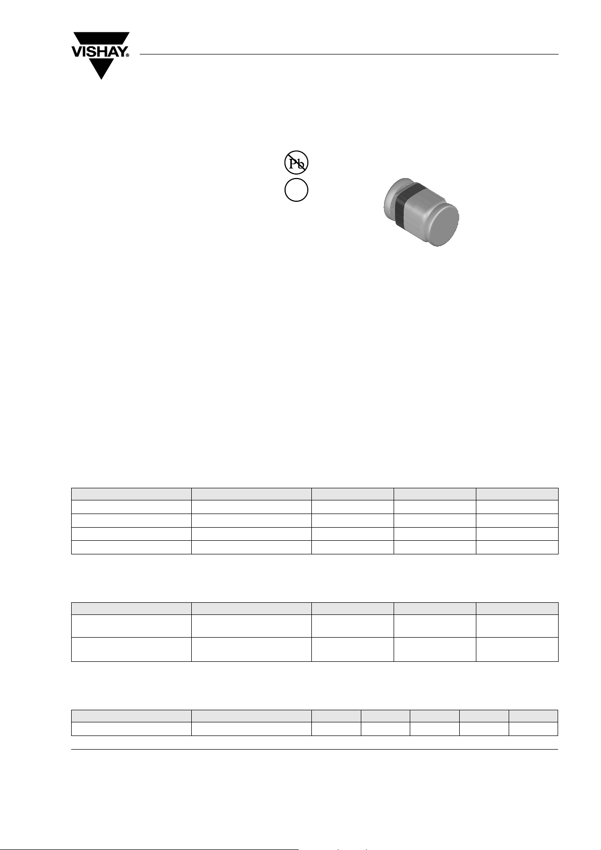
Case: MicroMELF
Weight: approx. 12 mg
Packaging codes/options:
TR / 2.5 k per 7" reel, 12.5 k/box
TR3 / 10 k per 13" reel, 10 k/box
Absolute Maximum Ratings
T
= 25 °C, unless otherwise specified
amb
Parameter Test condition Symbol Val ue Unit
Power dissipation R
Z-current I
Junction temperature T
Storage temperature range T
≤ 300 K/W P
thJA
Thermal Characteristics
T
= 25 °C, unless otherwise specified
amb
Parameter Test condition Symbol Val ue Unit
Junction to ambient air mounted on epoxy-glass hard
tissue, Fig. 1
Junction tie point
35 µm copper clad, 0.9 mm
copper area per electrode
2
V
Z
j
stg
R
thJA
R
thJL
500 mW
PV/V
Z
175 °C
- 65 to + 175 °C
500 K/W
300 K/W
mA
Electrical Characteristics
T
= 25 °C, unless otherwise specified
amb
Parameter Test condition Symbol Min Ty p. Max Unit
Forward voltage I
Document Number 85597
Rev. 1.9, 10-Mar-06
= 200 mA V
F
F
1.5 V
www.vishay.com
1
Page 2

BZM55-Series
Vishay Semiconductors
Electrical Characteristics
BZM55C..
Partnumber Zener Voltage
1)
Range
VZ at I
ZT
V Ω mA %/K mA µA V
min max min max
BZM55C2V4 2.28 2.56 < 85 < 600 5 - 0.09 - 0.06 1 < 50 < 100 1
BZM55C2V7 2.5 2.9 < 85 < 600 5 - 0.09 - 0.06 1 < 10 < 50 1
BZM55C3V0 2.8 3.2 < 90 < 600 5 - 0.08 - 0.05 1 < 4 < 40 1
BZM55C3V3 3.1 3.5 < 90 < 600 5 - 0.08 - 0.05 1 < 2 < 40 1
BZM55C3V6 3.4 3.8 < 90 < 600 5 -0.08 - 0.05 1 < 2 < 40 1
BZM55C3V9 3.7 4.1 < 90 < 600 5 - 0.08 - 0.05 1 < 2 < 40 1
BZM55C4V3 4 4.6 < 90 < 600 5 - 0.06 - 0.03 1 < 1 < 20 1
BZM55C4V7 4.4 5 < 80 < 600 5 - 0.05 0.02 1 < 0.5 < 10 1
BZM55C5V1 4.8 5.4 < 60 < 550 5 - 0.02 0.02 1 < 0.1 < 2 1
BZM55C5V6 5.2 6 < 40 < 450 5 - 0.05 0.05 1 < 0.1 < 2 1
BZM55C6V2 5.8 6.6 < 10 < 200 5 0.03 0.06 1 < 0.1 < 2 2
BZM55C6V8 6.4 7.2 < 8 < 150 5 0.03 0.07 1 < 0.1 < 2 3
BZM55C7V5 7 7.9 < 7 < 50 5 0.03 0.07 1 < 0.1 < 2 5
BZM55C8V2 7.7 8.7 < 7 < 50 5 0.03 0.08 1 < 0.1 < 2 6.2
BZM55C9V1 * 8.5 9.6 < 10 < 50 5 0.03 0.09 1 < 0.1 < 2 6.8
BZM55C10 * 9.4 0.6 < 15 < 70 5 0.03 0.1 1 < 0.1 < 2 7.5
BZM55C11 * 10.4 11.6 < 20 < 70 5 0.03 0.11 1 < 0.1 < 2 8.2
BZM55C12 * 11.4 12.7 < 20 < 90 5 0.03 0.11 1 < 0.1 < 2 9.1
BZM55C13 * 12.4 14.1 < 26 < 110 5 0.03 0.11 1 < 0.1 < 2 10
BZM55C15 * 13.8 15.6 < 30 < 110 5 0.03 0.11 1 < 0.1 < 2 11
BZM55C16 * 15.3 17.1 < 40 < 170 5 0.03 0.11 1 < 0.1 < 2 12
BZM55C18 * 16.8 19.1 < 50 < 170 5 0.03 0.11 1 < 0.1 < 2 13
BZM55C20 * 18.8 21.2 < 55 < 220 5 0.03 0.11 1 < 0.1 < 2 15
BZM55C22 * 20.8 23.3 < 55 < 220 5 0.04 0.12 1 < 0.1 < 2 16
BZM55C24 * 22.8 25.6 < 80 < 220 5 0.04 0.12 1 < 0.1 < 2 18
BZM55C27 * 25.1 28.9 < 80 < 220 5 0.04 0.12 1 < 0.1 < 2 20
BZM55C30 * 28 32 < 80 < 220 5 0.04 0.12 1 < 0.1 < 2 22
BZM55C33 * 31 35 < 80 < 220 5 0.04 0.12 1 < 0.1 < 2 24
BZM55C36 * 34 38 < 80 < 220 5 0.04 0.12 1 < 0.1 < 2 27
BZM55C39 * 37 41 < 90 < 500 2.5 0.04 0.12 0.5 < 0.1 < 5 30
BZM55C43 * 40 46 < 90 < 600 2.5 0.04 0.12 0.5 < 0.1 < 5 33
BZM55C47 * 44 50 110 < 700 2.5 0.04 0.12 0.5 < 0.1 < 5 36
BZM55C51 * 48 54 125 < 700 2.5 0.04 0.12 0.5 < 0.1 < 10 39
BZM55C56 * 52 60 135 < 1000 2.5 0.04 0.12 0.5 < 0.1 < 10 43
BZM55C62 * 58 66 150 < 1000 2.5 0.04 0.12 0.5 < 0.1 < 10 47
BZM55C68 * 64 72 200 < 1000 2.5 0.04 0.12 0.5 < 0.1 < 10 51
BZM55C75 * 70 79 250 < 1500 2.5 0.04 0.12 0.5 < 0.1 < 10 56
1)
tp ≤ 10 ms, T/tp > 1000
*)
Additionnal measurement of Voltage group 9V1 to 75 at 95 % V
Dynamic
Resistance
r
at
zjT
,
I
ZT
f = 1kHz
r
at
zjK
,
I
ZK
f = 1kHz
Te s t
Current
I
ZT
≤ 35 nA at Tj 25 °C
zmin
Temperature
Coefficient
TK
VZ
Te s t
Current
I
ZK
Reverse Leakage Current
I
R
at T
amb
= 25 °C
at T
= 150 °C
I
R
amb
at V
R
www.vishay.com
2
Document Number 85597
Rev. 1.9, 10-Mar-06
Page 3

BZM55-Series
Vishay Semiconductors
Electrical Characteristics
BZM55B..
Partnumber Zener Voltage
1)
Range
VZ at I
ZT
V Ω mA %/K mA µA V
min max min max
BZM55B2V4 2.35 2.45 < 85 < 600 5 - 0.09 - 0.06 1 < 50 < 100 1
BZM55B2V7 2.64 2.76 < 85 < 600 5 - 0.09 - 0.06 1 < 10 < 50 1
BZM55B3V0 2.94 3.06 < 90 < 600 5 - 0.08 - 0.05 1 < 4 < 40 1
BZM55B3V3 3.24 3.36 < 90 < 600 5 - 0.08 - 0.05 1 < 2 < 40 1
BZM55B3V6 3.52 3.68 < 90 < 600 5 - 0.08 - 0.05 1 < 2 < 40 1
BZM55B3V9 3.82 3.98 < 90 < 600 5 - 0.08 - 0.05 1 < 2 < 40 1
BZM55B4V3 4.22 4.38 < 90 < 600 5 - 0.06 - 0.03 1 < 1 < 20 1
BZM55B4V7 4.6 4.80 < 80 < 600 5 - 0.05 0.02 1 < 0.5 < 10 1
BZM55B5V1 5 5.20 < 60 < 550 5 - 0.02 0.02 1 < 0.1 < 2 1
BZM55B5V6 5.48 5.72 < 40 < 450 5 - 0.05 0.05 1 < 0.1 < 2 1
BZM55B6V2 6.08 6.32 < 10 < 200 5 0.03 0.06 1 < 0.1 < 2 2
BZM55B6V8 6.66 6.94 < 8 < 150 5 0.03 0.07 1 < 0.1 < 2 3
BZM55B7V5 7.35 7.65 < 7 < 50 5 0.03 0.07 1 < 0.1 < 2 5
BZM55B8V2 8.04 8.36 < 7 < 50 5 0.03 0.08 1 < 0.1 < 2 6.2
BZM55B9V1 * 8.92 9.28 < 10 < 50 5 0.03 0.09 1 < 0.1 < 2 6.8
BZM55B10 * 9.8 10.20 < 15 < 70 5 0.03 0.1 1 < 0.1 < 2 7.5
BZM55B11 * 10.78 11.22 < 20 < 70 5 0.03 0.11 1 < 0.1 < 2 8.2
BZM55B12 * 11.76 12.24 < 20 < 90 5 0.03 0.11 1 < 0.1 < 2 9.1
BZM55B13 * 12.74 13.26 < 26 < 110 5 0.03 0.11 1 < 0.1 < 2 10
BZM55B15 * 14.7 15.30 < 30 < 110 5 0.03 0.11 1 < 0.1 < 2 11
BZM55B16 * 15.7 16.30 < 40 < 170 5 0.03 0.11 1 < 0.1 < 2 12
BZM55B18 * 17.64 18.36 < 50 < 170 5 0.03 0.11 1 < 0.1 < 2 13
BZM55B20 * 19.6 20.40 < 55 < 220 5 0.03 0.11 1 < 0.1 < 2 15
BZM55B22 * 21.55 22.45 < 55 < 220 5 0.04 0.12 1 < 0.1 < 2 16
BZM55B24 * 23.5 24.5 < 80 < 220 5 0.04 0.12 1 < 0.1 < 2 18
BZM55B27 * 26.4 27.6 < 80 < 220 5 0.04 0.12 1 < 0.1 < 2 20
BZM55B30 * 29.4 30.6 < 80 < 220 5 0.04 0.12 1 < 0.1 < 2 22
BZM55B33 * 32.4 33.6 < 80 < 220 5 0.04 0.12 1 < 0.1 < 2 24
BZM55B36 * 35.3 36.7 < 80 < 220 5 0.04 0.12 1 < 0.1 < 2 27
BZM55B39 * 38.2 39.8 < 90 < 500 2.5 0.04 0.12 1 < 0.1 < 5 30
BZM55B43 * 42.1 43.9 < 90 < 600 2.5 0.04 0.12 0.5 < 0.1 < 5 33
BZM55B47 * 46.1 47.9 < 110 < 700 2.5 0.04 0.12 0.5 < 0.1 < 5 36
BZM55B51 * 50 52.0 < 125 < 700 2.5 0.04 0.12 0.5 < 0.1 < 10 39
BZM55B56 * 54.9 57.1 < 135 < 1000 2.5 0.04 0.12 0.5 < 0.1 < 10 43
BZM55B62 * 60.8 63.2 < 150 < 1000 2.5 0.04 0.12 0.5 < 0.1 < 10 47
BZM55B68 * 66.6 69.4 < 200 < 1000 2.5 0.04 0.12 0.5 < 0.1 < 10 51
BZM55C75 * 73.5 76.5 < 250 < 1500 2.5 0.04 0.12 0.5 < 0.1 < 10 56
1)
tp ≤ 10 ms, T/tp > 1000
*)
Additionnal measurement of Voltage group 9V1 to 75 at 95 % V
Dynamic
Resistance
r
at
zjT
,
I
ZT
f = 1kHz
r
at
zjK
,
I
ZK
f = 1kHz
Te st
Current
I
ZT
≤ 35 nA at Tj 25 °C
zmin
Temperature
Coefficient
TK
VZ
Te s t
Current
I
ZK
Reverse Leakage Current
IR at
T
amb
25 °C
=
IR at
T
amb
150 °C
=
at V
R
Document Number 85597
Rev. 1.9, 10-Mar-06
www.vishay.com
3
Page 4

BZM55-Series
Vishay Semiconductors
Typical Characteristics
T
= 25 °C, unless otherwise specified
amb
600
500
400
300
200
100
- Total Power Dissipation (mW)
tot
0
P
0 120 160
95 9602
T
amb
80
40
- Ambient Temperature (°C)
200
Figure 1. Total Power Dissipation vs. Ambient Temperature
1000
Tj = 25 °C
100
= 5 mA
I
Z
10
- Voltage Change (mV)
Z
V
95 9598
1
0
10 15 20
5
VZ - Z-Voltage (V)
25
Figure 2. Typical Change of Working Voltage under Operating
Conditions at T
amb
=25°C
200
150
VR = 2 V
100
Tj = 25 °C
50
- Diode Capacitance (pF)
D
C
0
20
25
95 9601
5
10 15
0
VZ - Z-Voltage (V)
Figure 4. Diode Capacitance vs. Z-Voltage
1.3
V
= VZt/VZ (25 °C)
Ztn
1.2
1.1
1.0
0.9
- Relative Voltage Change
Ztn
V
0.8
- 60 60 120 180
95 9599
TKVZ = 10 x 10-4/K
8 x 10⁻⁴/K
6 x 10
4 x 10
2 x 10
0
- 2 x 10⁻⁴/K
- 4 x 10⁻⁴/K
0
Tj - Junction Temperature (°C)
-4
/K
-4
/K
-4
/K
240
Figure 5. Typical Change of Working Voltage vs. Junction
Temperature
/K)
15
-4
(10
Z
10
5
IZ = 5 mA
0
- 5
- Temperature Coefficient of V
TK
VZ
95 9600
0
10 20
V
- Z-Voltage (V)
Z
30
Figure 3. Temperature Coefficient of Vz vs. Z-Voltage
www.vishay.com
4
40
50
100
10
1
Tj = 25 °C
0.1
0.01
- Forward Current (mA)
F
I
0.001
0 0.2 0.4 0.6 0.8
95 9605
VF - Forward Voltage (V)
Figure 6. Forward Current vs. Forward Voltage
Document Number 85597
Rev. 1.9, 10-Mar-06
1.0
Page 5

BZM55-Series
Vishay Semiconductors
100
80
60
40
- Z-Current (mA)
Z
I
20
0
046
95 9604
VZ - Z-Voltage (V)
Figure 7. Z-Current vs. Z-Voltage
50
40
30
20
- Z-Current (mA)
Z
I
10
P
T
8
P
tot
T
amb
= 500 mW
tot
= 25 °C
amb
12
= 500 mW
= 25 °C
20
0.152
25
10
95 10329
Figure 10. Board for R
Reflow Soldering
1.2
0.8 0.8
0.71 1.3
0.355
2.5
24
definition (in mm)
thJA
0.8
1.27
9.9
0
15 20 25 30
95 9607
VZ - Z-Voltage (V)
35
Figure 8. Z-Current vs. Z-Voltage
1000
(Ω)
IZ = 1 mA
100
5 mA
10 mA
10
- Differential Z-Resistance
Z
1
r
0 5 10 15 20
95 9606
VZ - Z-Voltage (V)
Tj = 25 °C
25
Figure 9. Differential Z-Resistance vs. Z-Voltage
16773
2.4
Figure 11. Recommended foot pads (in mm)
Wave Soldering
1.4
0.9 0.9
16774
Figure 12. Recommended foot pads (in mm)
1.0
2.8
Document Number 85597
Rev. 1.9, 10-Mar-06
www.vishay.com
5
Page 6

BZM55-Series
Vishay Semiconductors
1000
tP/T = 0.5
tP/T = 0.1
1
-1
10
tP/T = 0.2
tP/T = 0.05
tP/T = 0.02
10
tP/T = 0.01
0
tP - Pulse Length (ms)
Figure 13. Thermal Response
100
10
- Thermal Resistance for Pulse Cond. (KW)
thp
Z
95 9603
Package Dimensions in mm (Inches)
Single Pulse
iZM = (- VZ + (V
1
10
2
+ 4rzj x T/Z
Z
10
R
T = T
2
thJA
= 300 K/W
- T
jmax
1/2
)
)/(2rzj)
thp
amb
Cathode indification
Glass case
MicroMELF
1 (0.039) surface plan
1.2 (0.047)
0.25 (0.010)
0.15 (0.006)
2.0 (0.079)
1.8 (0.071)
Reflow Soldering
1.2 (0.047)
0.8 (0.031) 0.8 (0.031)
0.8 (0.031)
2.4 (0.094)
Document No.: 6.560-5007.01-4
Rev. 11, 07.Feb.2005
9612072
)
Glass
< 1.35 (0.053
surface plan
0.6
1.1 (0.043)
> R 2.5 (R 0.098)
Glass
ISO Method E
Wave Soldering
1.4 (0.055)
0.9 (0.035) 0.9 (0.035)
1.0 (0.039)
2.8 (0.110)
(0.024)
www.vishay.com
6
Document Number 85597
Rev. 1.9, 10-Mar-06
Page 7

BZM55-Series
Vishay Semiconductors
Ozone Depleting Substances Policy Statement
It is the policy of Vishay Semiconductor GmbH to
1. Meet all present and future national and international statutory requirements.
2. Regularly and continuously improve the performance of our products, processes, distribution and operating
systems with respect to their impact on the health and safety of our employees and the public, as well as
their impact on the environment.
It is particular concern to control or eliminate releases of those substances into the atmosphere which are
known as ozone depleting substances (ODSs).
The Montreal Protocol (1987) and its London Amendments (1990) intend to severely restrict the use of ODSs
and forbid their use within the next ten years. Various national and international initiatives are pressing for an
earlier ban on these substances.
Vishay Semiconductor GmbH has been able to use its policy of continuous improvements to eliminate the use
of ODSs listed in the following documents.
1. Annex A, B and list of transitional substances of the Montreal Protocol and the London Amendments
respectively
2. Class I and II ozone depleting substances in the Clean Air Act Amendments of 1990 by the Environmental
Protection Agency (EPA) in the USA
3. Council Decision 88/540/EEC and 91/690/EEC Annex A, B and C (transitional substances) respectively.
Vishay Semiconductor GmbH can certify that our semiconductors are not manufactured with ozone depleting
substances and do not contain such substances.
We reserve the right to make changes to improve technical design
and may do so without further notice.
Parameters can vary in different applications. All operating parameters must be validated for each
customer application by the customer. Should the buyer use Vishay Semiconductors products for any
unintended or unauthorized application, the buyer shall indemnify Vishay Semiconductors against all
claims, costs, damages, and expenses, arising out of, directly or indirectly, any claim of personal
damage, injury or death associated with such unintended or unauthorized use.
Vishay Semiconductor GmbH, P.O.B. 3535, D-74025 Heilbronn, Germany
Document Number 85597
Rev. 1.9, 10-Mar-06
www.vishay.com
7
Page 8

Legal Disclaimer Notice
Vishay
Notice
Specifications of the products displayed herein are subject to change without notice. Vishay Intertechnology, Inc.,
or anyone on its behalf, assumes no responsibility or liability for any errors or inaccuracies.
Information contained herein is intended to provide a product description only. No license, express or implied, by
estoppel or otherwise, to any intellectual property rights is granted by this document. Except as provided in Vishay's
terms and conditions of sale for such products, Vishay assumes no liability whatsoever, and disclaims any express
or implied warranty, relating to sale and/or use of Vishay products including liability or warranties relating to fitness
for a particular purpose, merchantability, or infringement of any patent, copyright, or other intellectual property right.
The products shown herein are not designed for use in medical, life-saving, or life-sustaining applications.
Customers using or selling these products for use in such applications do so at their own risk and agree to fully
indemnify Vishay for any damages resulting from such improper use or sale.
Document Number: 91000 www.vishay.com
Revision: 08-Apr-05 1
 Loading...