Page 1

BCR
Vishay Electro-Films
Thin Film, Back-Contact Resistor
CHIP
RESISTORS
Product may not
be to scale
The Back Contact Resistor (BCR) series single-value
back-contact resistor chip is one of the smallest chips available.
The BCR requires only one wire bond thus saving hybrid space.
The BCRs are manufactured using Vishay Electro-Films
(EFI) sophisticated thin film equipment and manufacturing
technology. The BCRs are 100 % electrically tested and
visually inspected to MIL-STD-883.
• Wire bondable
• Only one wire bond required
• Small size: 0.020 inches square.
• Resistance range: 10 Ω to 1 MΩ
• Oxidized silicon substrate for good power dissipation
• Resistor material: Tantalum nitride, self-passivating
• Moisture resistant
APPLICATIONS
FEATURES
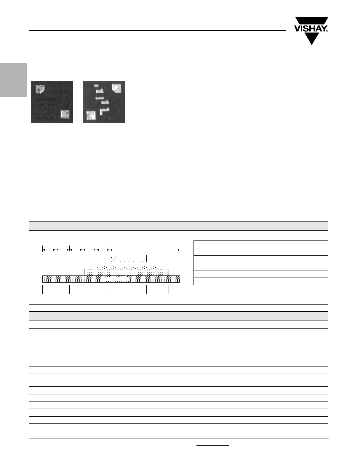
Vishay EFI BCR resistor chips are widely used in hybrid packages where space is limited. The bottom connection is made by
attaching the back of the chip to the substrate either eutectically or with conductive epoxy. The single wire bond is made to the
notched pad on the top of the chip. (The other rectangular pad on the top of the chip is a via hole, a low-ohmic contact connecting
the resistor to the bottom of the chip.)
TEMPERATURE COEFFICIENT OF RESISTANCE, VALUES AND TOLERANCES
Tightest Standard Tolerance Available
0.5 %1 %2 %5 %
0.2 %
± 100 ppm/°C
± 250 ppm/°C
20 Ω 50 Ω 200 Ω 1 kΩ
100 Ω10 Ω
± 25 ppm/°C
± 50 ppm/°C
0.1 %
200 kΩ
360 kΩ
620 kΩ
1 MΩ
CLASS H* CLASS K*
010 056
002 061
027 059
008 052
*MIL-PRF-38534 inspection criteria
PROCESS CODE
STANDARD ELECTRICAL SPECIFICATIONS
PARAMETER
Noise, MIL-STD-202, Method 308
100 Ω - 250 kΩ
< 100 Ω or > 251 kΩ
Moisture resistance, MIL-STD-202
Method 106
Stability, 1000 h, + 125 °C, 125 mW ± 1.0 % max. ΔR/R
Operating Temperature Range - 55 °C to + 125 °C
Thermal Shock, MIL-STD-202,
Method 107, Test Condition F
High Temperature Exposure, + 150 °C, 100 h ± 0.5 % max. ΔR/R
Dielectric Voltage Breakdown 200 V
Insulation Resistance 10
Operating Voltage 75 V max.
DC Power Rating at + 70 °C (Derated to Zero at + 175 °C) 250 mW
5 x Rated Power Short-Time Overload, + 25 °C, 5 s ± 0.25 % max. ΔR/R
www.vishay.com For technical questions, contact: efi@vishay.com
54 Revision: 12-Mar-08
- 35 dB typ.
- 20 dB typ.
± 0.5 % max. ΔR/R
± 0.25 % max. ΔR/R
12
min.
Document Number: 61023
Page 2

BCR
Thin Film, Back-Contact Resistor
Vishay Electro-Films
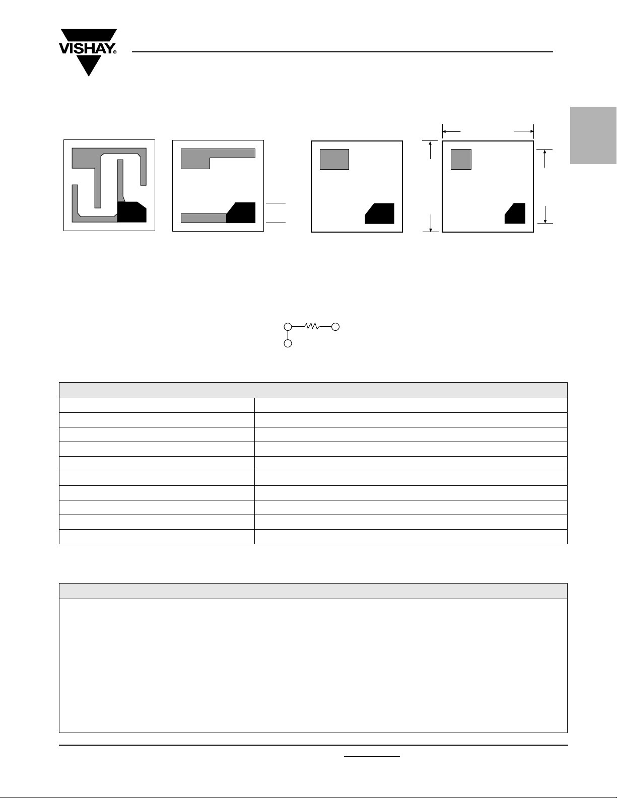
DIMENSIONS in inches
0.020
0.004
TYPICAL RANGE
10 Ω - 23 Ω
Note:
• Notched shaded area represents top bonding pad. The backside of the chip constitutes the second resistor connection.
TYPICAL RANGE
24 Ω - 220 Ω
TYPICAL RANGE
1
80 Ω - 2.2 kΩ
TYPICAL RANGE
1.6 kΩ - 1 MΩ
SCHEMATIC
Bond Pad
Back of Chip
RESISTORS
CHIP
0.020
0.016
MECHANICAL SPECIFICATIONS in inches
PARAMETER
Chip Size 0.020 x 0.020 ± 0.002 (0.50 x 0.50 ± 0.05 mm)
Chip Thickness 0.010 ± 0.003 (0.253 ± 0.05 mm)
Chip Substrate Material Oxidized silicon, 10 kÅ minimum SiO
Resistor Material Tantalum nitride, self-passivating
Bonding Pad Size 0.004 x 0.004 (0.100 x 0.100 mm)
Number of Pads 1
Pad Material 10 kÅ minimum aluminum
Backing 3 kÅ minimum gold
Recommended Attachment Method Eutectic or conductive epoxy
Options: Gold bonding pads, 15 kÅ minimum thickness
Consult Applications Engineer
2
ORDERING INFORMATION
Example: 100 % visual, 16 kΩ, ± 1 %, ± 250 ppm/°C TCR, aluminum pads, class H visual inspection
W
INSPECTION/
PA CK A GI N G
W = 100 % visually inspected
parts in matrix tray per
MIL-STD-883
X = Sample, visually inspected
parts loaded in matrix trays
(4 % AQL)
Document Number: 61023 For technical questions, contact: efi@vishay.com
Revision: 12-Mar-08 55
BCR
PRODUCT
FAM ILY
008
PROCESS
CODE
See Process Code
table
significant digits of the
1600
RESISTANCE
VAL UE
Use first 4 digits
resistance
1
MULTIPLIER
CODE
B = 0.01
A = 0.1
0 = 1
1 = 10
2 = 100
3 = 1000
F
TOLERANCE
CODE
B = 0.1 %
C = 0.2 %
D = 0.5 %
F = 1.0 %
G = 2.0 %
H = 2.5 %
J = 5.0 %
K = 10 %
www.vishay.com
Page 3

Legal Disclaimer Notice
Vishay
Disclaimer
All product specifications and data are subject to change without notice.
Vishay Intertechnology, Inc., its affiliates, agents, and employees, and all persons acting on its or their behalf
(collectively, “Vishay”), disclaim any and all liability for any errors, inaccuracies or incompleteness contained herein
or in any other disclosure relating to any product.
Vishay disclaims any and all liability arising out of the use or application of any product described herein or of any
information provided herein to the maximum extent permitted by law. The product specifications do not expand or
otherwise modify Vishay’s terms and conditions of purchase, including but not limited to the warranty expressed
therein, which apply to these products.
No license, express or implied, by estoppel or otherwise, to any intellectual property rights is granted by this
document or by any conduct of Vishay.
The products shown herein are not designed for use in medical, life-saving, or life-sustaining applications unless
otherwise expressly indicated. Customers using or selling Vishay products not expressly indicated for use in such
applications do so entirely at their own risk and agree to fully indemnify Vishay for any damages arising or resulting
from such use or sale. Please contact authorized Vishay personnel to obtain written terms and conditions regarding
products designed for such applications.
Product names and markings noted herein may be trademarks of their respective owners.
Document Number: 91000 www.vishay.com
Revision: 18-Jul-08 1
 Loading...