

www.vishay.com
Small Signal Zener Diodes, Dual
2
PRIMARY CHARACTERISTICS
PARAMETER VALUE UNIT
range nom. 2.7 to 51 V
V
Z
Test current I
specification Pulse current
V
Z
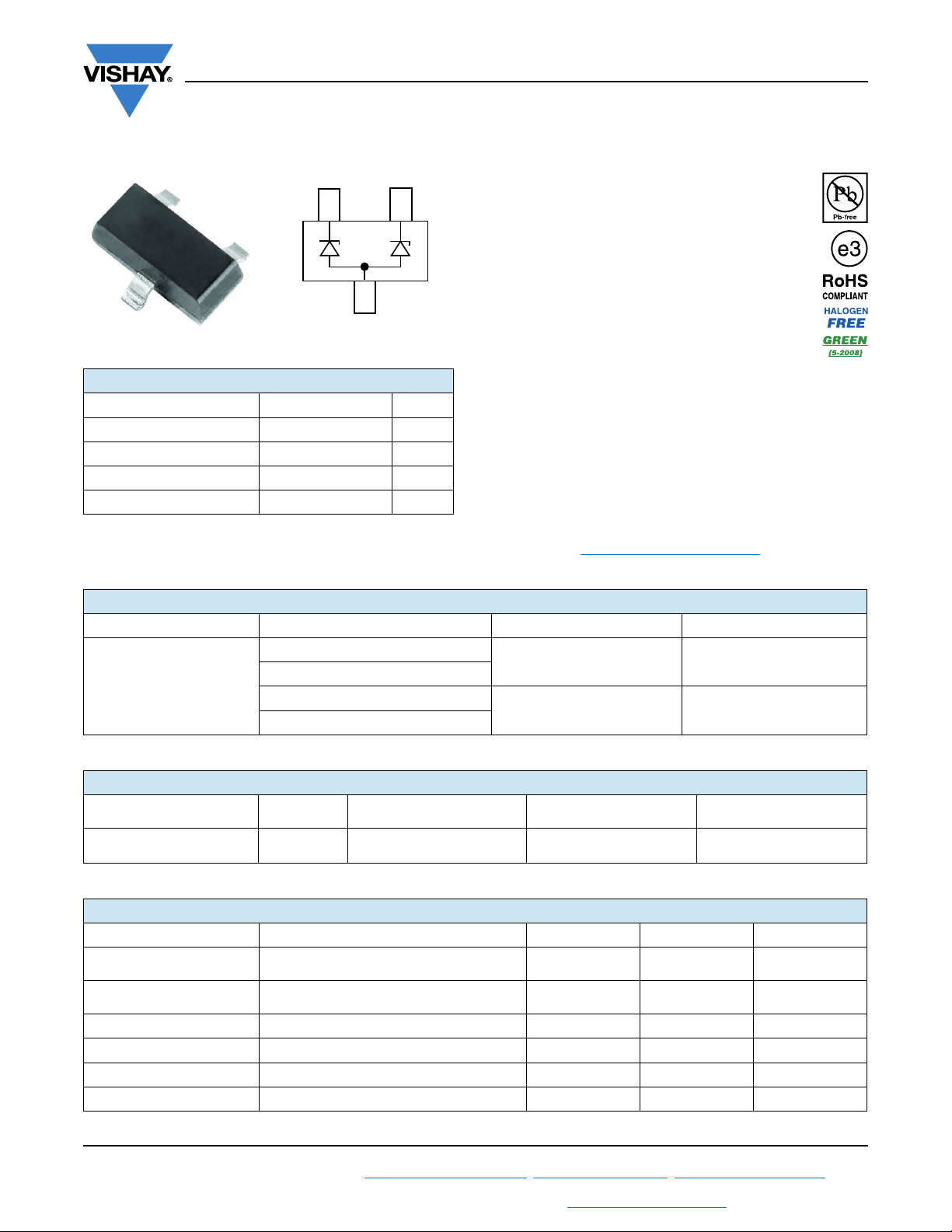
Int. construction Dual common anode
5mA
ZT
1
3
20456
AZ23-G-Series
Vishay Semiconductors
FEATURES
• Dual silicon planar Zener diodes, common
anode
• The Zener voltages are graded according to the
international E24 standard. Standard Zener
voltage tolerance is ± 5 %, indicated by the “C”
in the ordering code. Replace “C” with “B” for
2 % tolerance.
• The parameters are valid for both diodes in one
case. V
is 5 %
• AEC-Q101 qualified
• ESD capability according to AEC-Q101:
Human body model > 8 kV
Machine model > 800 V
• Base P/N-G3 - green, commercial grade
• Base P/N-HG3 - green, AEC-Q101 qualified
(part number available on request)
• Material categorization: For definitions of compliance
please see www.vishay.com/doc?99912
and Rzj of the two diodes in one case
Z
ORDERING INFORMATION
DEVICE NAME ORDERING CODE TAPED UNITS PER REEL MINIMUM ORDER QUANTITY
AZ23-G-series
AZ23C2V7-G3-08 to AZ23C51-G3-08
AZ23B2V7-G3-08 to AZ23B51-G3-08
AZ23C2V7-G3-18 to AZ23C51-G3-18
AZ23B2V7-G3-18 to AZ23B51-G3-18
3000 (8 mm tape on 7" reel) 15 000
10 000 (8 mm tape on 13" reel) 10 000
PACKAGE
PACKAGE NAME WEIGHT
SOT-23 8.1 mg UL 94 V-0
ABSOLUTE MAXIMUM RATINGS (T
PARAMETER TEST CONDITION SYMBOL VALUE UNIT
Power dissipation
Thermal resistance, junction
to ambient air
Junction temperature
Storage temperature range
Zener current I
Operating temperature range
Device on fiberglass substrate,
Device on fiberglass substrate,
MOLDING COMPOUND
FLAMMABILITY RATING
= 25 °C, unless otherwise specified)
amb
see layout on page 6
see layout on page 6
MOISTURE SENSITIVITY
LEVEL
MSL level 1
(according J-STD-020)
P
tot
R
thJA
T
j
T
stg
Z
T
op
-65 to +150 °C
-55 to +150 °C
SOLDERING CONDITIONS
260 °C/10 s at terminals
300 mW
420 K/W
150 °C
P
tot/VZ
mA
Rev. 1.4, 04-Mar-14
For technical questions within your region: DiodesAmericas@vishay.com
THIS DOCUMENT IS SUBJECT TO CHANGE WITHOUT NOTICE. THE PRODUCTS DESCRIBED HEREIN AND THIS DOCUMENT
ARE SUBJECT TO SPECIFIC DISCLAIMERS, SET FORTH AT www.vishay.com/doc?91000
1
, DiodesAsia@vishay.com, DiodesEurope@vishay.com
Document Number: 85867

www.vishay.com
AZ23-G-Series
Vishay Semiconductors
ELECTRICAL CHARACTERISTICS (T
ZENER VOLTAGE
RANGE
VZ at I
ZT1
PART NUMBER
MARKING
CODE
= 25 °C, unless otherwise specified)
amb
(1)
TEST
CURRENT
I
ZT1
I
ZT2
REVERSE
VOLTAGE
VR at I
DYNAMIC
RESISTANCE
ZZ at I
R
ZT1ZZK
at I
TEMPERATURE
COEFFICIENT OF
ZENER VOLTAGE
ZT2
VZ at I
V mA V nA 10-4/°C
MIN. NOM. MAX. MIN. MAX.
AZ23C2V7-G D41 2.5 2.7 2.9 5 1 - - 75 (< 83) < 500 -9 -4
AZ23C3V0-G D42 2.8 3.0 3.2 5 1 - - 80 (< 95) < 500 -9 -3
AZ23C3V3-G D43 3.1 3.3 3.5 5 1 - - 80 (< 95) < 500 -8 -3
AZ23C3V6-G D44 3.4 3.6 3.8 5 1 - - 80 (< 95) < 500 -8 -3
AZ23C3V9-G D45 3.7 3.9 4.1 5 1 - - 80 (< 95) < 500 -7 -3
AZ23C4V3-G D46 4 4.3 4.6 5 1 - - 80 (< 95) < 500 -6 -1
AZ23C4V7-G D47 4.4 4.7 5 5 1 - - 70 (< 78) < 500 -5 2
AZ23C5V1-G D48 4.8 5.1 5.4 5 1 > 0.8 100 30 (< 60) < 480 -3 4
AZ23C5V6-G D49 5.2 5.6 6 5 1 > 1 100 10 (< 40) < 400 -2 6
AZ23C6V2-G D50 5.8 6.2 6.6 5 1 > 2 100 4.8 (< 10) < 200 -1 7
AZ23C6V8-G D51 6.4 6.8 7.2 5 1 > 3 100 4.5 (< 8) < 150 2 7
AZ23C7V5-G D52 7 7.5 7.9 5 1 > 5 100 4 (< 7) < 50 3 7
AZ23C8V2-G D53 7.7 8.2 8.7 5 1 > 6 100 4.5 (< 7) < 50 4 7
AZ23C9V1-G D54 8.5 9.1 9.6 5 1 > 7 100 4.8 (< 10) < 50 5 8
AZ23C10-G D55 9.4 10 10.6 5 1 > 7.5 100 5.2 (< 15) < 70 5 8
AZ23C11-G D56 10.4 11 11.6 5 1 > 8.5 100 6 (< 20) < 70 5 9
AZ23C12-G D57 11.4 12 12.7 5 1 > 9 100 7 (< 20) < 90 6 9
AZ23C13-G D58 12.4 13 14.1 5 1 > 10 100 9 (< 25) < 110 7 9
AZ23C15-G D59 13.8 15 15.6 5 1 > 11 100 11 (< 30) < 110 7 9
AZ23C16-G D60 15.3 16 17.1 5 1 > 12 100 13 (< 40) < 170 8 9.5
AZ23C18-G D61 16.8 18 19.1 5 1 > 14 100 18 (< 50) < 170 8 9.5
AZ23C20-G D62 18.8 20 21.2 5 1 > 15 100 20 (< 50) < 220 8 10
AZ23C22-G D63 20.8 22 23.3 5 1 > 17 100 25 (< 55) < 220 8 10
AZ23C24-G D64 22.8 24 25.6 5 1 > 18 100 28 (< 80) < 220 8 10
AZ23C27-G D65 25.1 27 28.9 5 1 > 20 100 30 (< 80) < 250 8 10
AZ23C30-G D66 28 30 32 5 1 > 22.5 100 35 (< 80) < 250 8 10
AZ23C33-G D67 31 33 35 5 1 > 25 100 40 (< 80) < 250 8 10
AZ23C36-G D68 34 36 38 5 1 > 27 100 40 (< 90) < 250 8 10
AZ23C39-G D69 37 39 41 5 1 > 29 100 50 (< 90) < 300 10 12
AZ23C43-G D70 40 43 46 5 1 > 32 100 60 (< 100) < 700 10 12
AZ23C47-G D71 44 47 50 5 1 > 35 100 70 (< 100) < 750 10 12
AZ23C51-G D72 48 51 50 5 1 > 38 100 70 (< 100) < 750 10 12
Note
(1)
Tested with pulses tp = 5 ms
ZT
Rev. 1.4, 04-Mar-14
For technical questions within your region: DiodesAmericas@vishay.com
THIS DOCUMENT IS SUBJECT TO CHANGE WITHOUT NOTICE. THE PRODUCTS DESCRIBED HEREIN AND THIS DOCUMENT
ARE SUBJECT TO SPECIFIC DISCLAIMERS, SET FORTH AT www.vishay.com/doc?91000
2
, DiodesAsia@vishay.com, DiodesEurope@vishay.com
Document Number: 85867
www.vishay.com
AZ23-G-Series
Vishay Semiconductors
ELECTRICAL CHARACTERISTICS (T
ZENER VOLTAGE
RANGE
VZ at I
ZT1
PART NUMBER
MARKING
CODE
= 25 °C, unless otherwise specified)
amb
(1)
TEST
CURRENT
I
ZT1
I
ZT2
REVERSE
VOLTAGE
VR at I
DYNAMIC
RESISTANCE
ZZ at I
R
ZT1ZZK
at I
TEMPERATURE
COEFFICIENT OF
ZENER VOLTAGE
ZT2
VZ at I
V mA V nA 10-4/°C
MIN. NOM. MAX. MIN. MAX.
AZ23B2V7-G D41 2.65 2.7 2.75 5 1 - - 75 (< 83) < 500 -9 -4
AZ23B3V0-G D42 2.94 3.0 3.06 5 1 - - 80 (< 95) < 500 -9 -3
AZ23B3V3-G D43 3.23 3.3 3.37 5 1 - - 80 (< 95) < 500 -8 -3
AZ23B3V6-G D44 3.53 3.6 3.67 5 1 - - 80 (< 95) < 500 -8 -3
AZ23B3V9-G D45 3.82 3.9 3.98 5 1 - - 80 (< 95) < 500 -7 -3
AZ23B4V3-G D46 4.21 4.3 4.39 5 1 - - 80 (< 95) < 500 -6 -1
AZ23B4V7-G D47 4.61 4.7 4.79 5 1 - - 70 (< 78) < 500 -5 2
AZ23B5V1-G D48 5 5.1 5.2 5 1 > 0.8 100 30 (< 60) < 480 -3 4
AZ23B5V6-G D49 5.49 5.6 5.71 5 1 > 1 100 10 (< 40) < 400 -2 6
AZ23B6V2-G D50 6.08 6.2 6.32 5 1 > 2 100 4.8 (< 10) < 200 -1 7
AZ23B6V8-G D51 6.66 6.8 6.94 5 1 > 3 100 4.5 (< 8) < 150 2 7
AZ23B7V5-G D52 7.35 7.5 7.65 5 1 > 5 100 4 (< 7) < 50 3 7
AZ23B8V2-G D53 8.04 8.2 8.36 5 1 > 6 100 4.5 (< 7) < 50 4 7
AZ23B9V1-G D54 8.92 9.1 9.28 5 1 > 7 100 4.8 (< 10) < 50 5 8
AZ23B10-G D55 9.8 10 10.2 5 1 > 7.5 100 5.2 (< 15) < 70 5 8
AZ23B11-G D56 10.8 11 11.2 5 1 > 8.5 100 6 (< 20) < 70 5 9
AZ23B12-G D57 11.8 12 12.2 5 1 > 9 100 7 (< 20) < 90 6 9
AZ23B13-G D58 12.7 13 13.3 5 1 > 10 100 9 (< 25) < 110 7 9
AZ23B15-G D59 14.7 15 15.3 5 1 > 11 100 11 (< 30) < 110 7 9
AZ23B16-G D60 15.7 16 16.3 5 1 > 12 100 13 (< 40) < 170 8 0.5
AZ23B18-G D61 17.6 18 18.4 5 1 > 14 100 18 (< 50) < 170 8 0.5
AZ23B20-G D62 19.6 20 20.4 5 1 > 15 100 20 (< 50) < 220 8 10
AZ23B22-G D63 21.6 22 22.4 5 1 > 17 100 25 (< 55) < 220 8 10
AZ23B24-G D64 23.5 24 24.5 5 1 > 18 100 28 (< 80) < 220 8 10
AZ23B27-G D65 26.5 27 27.5 5 1 > 20 100 30 (< 80) < 250 8 10
AZ23B30-G D66 29.4 30 30.6 5 1 > 22.5 100 35 (< 80) < 250 8 10
AZ23B33-G D67 32.3 33 33.7 5 1 > 25 100 40 (< 80) < 250 8 10
AZ23B36-G D68 35.3 36 36.7 5 1 > 27 100 40 (< 90) < 250 8 10
AZ23B39-G D69 38.2 39 39.8 5 1 > 29 100 50 (< 90) < 300 10 12
AZ23B43-G D70 42.1 43 43.9 5 1 > 32 100 60 (< 100) < 700 10 12
AZ23B47-G D71 46.1 47 47.9 5 1 > 35 100 70 (< 100) < 750 10 12
AZ23B51-G D72 50 51 52 5 1 > 38 100 70 (< 100) < 750 10 12
Note
(1)
Tested with pulses tp = 5 ms
ZT
Rev. 1.4, 04-Mar-14
For technical questions within your region: DiodesAmericas@vishay.com
THIS DOCUMENT IS SUBJECT TO CHANGE WITHOUT NOTICE. THE PRODUCTS DESCRIBED HEREIN AND THIS DOCUMENT
ARE SUBJECT TO SPECIFIC DISCLAIMERS, SET FORTH AT www.vishay.com/doc?91000
3
, DiodesAsia@vishay.com, DiodesEurope@vishay.com
Document Number: 85867

www.vishay.com
18114
mA
10
3
10
2
10
-1
10
-2
10
-3
10
-4
10
-5
10
1
I
F
V
F
0 0.2 0.4 0.6 0.8 1V
TJ = 100 °C
T
J
= 25 °C
18115
mW
400
100
0
300
200
P
tot
T
amb
0 100 200 °C
500
18121
10
3
5
4
3
2
5
4
3
2
10
2
1
R
zth
5
4
3
2
10
Ω
1
2345 2345
10 100 V
VZ at IZ = 5 mA
negative
positive
ΔΔV
Z
T
j
R
zth
= R
thA
x VZ x
18122
100
7
5
4
3
2
7
5
4
3
2
1
Ω
R
zj
10
T
j
= 25 °C
I
Z
= 5 mA
1
2345 2345
10 100 V
V
Z
18123
Δ
25
20
15
10
5
0
- 5
mV/°C
Δ
V
Z
T
j
1
2345 2345
10 100 V
V
Z
5 mA
1 mA
20 mA
I
Z
=
AZ23-G-Series
Vishay Semiconductors
TYPICAL CHARACTERISTICS (T
Fig. 1 - Forward Characteristics
= 25 °C, unless otherwise specified)
amb
Fig. 4 - Thermal Differential Resistance vs. Zener Voltage
Fig. 2 - Admissible Power Dissipation vs. Ambient Temperature
Ω
3
10
7
5
4
R
3
zj
2
2
10
7
5
4
3
Rev. 1.4, 04-Mar-14
2
10
18120
Fig. 3 - Dynamic Resistance vs. Zener Current
For technical questions within your region: DiodesAmericas@vishay.com
THIS DOCUMENT IS SUBJECT TO CHANGE WITHOUT NOTICE. THE PRODUCTS DESCRIBED HEREIN AND THIS DOCUMENT
47 + 51
43
39
36
0.1
2345 2345
110
ARE SUBJECT TO SPECIFIC DISCLAIMERS, SET FORTH AT www.vishay.com/doc?91000
I
Z
Tj = 25 °C
mA
Fig. 5 - Dynamic Resistance vs. Zener Voltage
Fig. 6 - Temperature Dependence of Zener Voltage vs.
Zener Voltage
4
Document Number: 85867
, DiodesAsia@vishay.com, DiodesEurope@vishay.com

www.vishay.com
18124
VZ at IZ = 5 mA
25
15
10
8
7
6.2
5.9
5.6
5.1
4.7
3.6
0.8
0.7
0.6
0.5
0.4
0.3
0.2
0.1
0
- 1
- 0.2
V
Z
V
T
j
020406080
100 120 140 C
Δ
18125
Δ
100
80
60
40
20
0
mV/°C
Δ
V
Z
T
j
0
20 40 80
60 100 V
V
Z
IZ = 5 mA
18126
Δ
9
7
5
3
1
- 1
V
V
Z
8
6
4
2
0
0
100
60
T
j
20 40 120
80 140 °C
I
Z
= 2 mA
51
43
36
Δ
V
Z
18127
1.6
1.4
1.2
0.8
0.6
0.4
0.2
- 0.2
- 0.4
Vishay Semiconductors
V
VZ = R
x I
Δ
zth
Z
1
0
1
2345 2345
AZ23-G-Series
10 100 V
VZ at IZ = 5 mA
Fig. 7 - Change of Zener Voltage vs. Junction Temperature
Fig. 8 - Temperature Dependence of Zener Voltage vs.
Zener Voltage
Fig. 10 - Change of Zener Voltage from Turn-on up to the Point of
Thermal Equilibrium vs. Zener Voltage
V
5
Δ
= R
x I
V
Z
zth
Z
4
Δ
V
Z
3
IZ = 5 mA
2
0
18128
1
0
20 40 60 80
= 2 mA
I
Z
V
Z
100 V
Fig. 11 - Change of Zener Voltage from Turn-on up to the Point of
Thermal Equilibrium vs. Zener Voltage
mA
50
Tj = 25 °C
40
l
Z
2.7
3.3
3.9
4.7
5.6
6.8
8.2
30
20
Test
current
10
5 mA
Fig. 9 - Change of Zener Voltage vs. Junction Temperature
Rev. 1.4, 04-Mar-14
THIS DOCUMENT IS SUBJECT TO CHANGE WITHOUT NOTICE. THE PRODUCTS DESCRIBED HEREIN AND THIS DOCUMENT
For technical questions within your region: DiodesAmericas@vishay.com
ARE SUBJECT TO SPECIFIC DISCLAIMERS, SET FORTH AT www.vishay.com/doc?91000
5
, DiodesAsia@vishay.com, DiodesEurope@vishay.com
I
Z
0
1
0 10 V
23456789
18111
V
Z
Fig. 12 - Breakdown Characteristics
Document Number: 85867

www.vishay.com
18112
10 20 30
0 40 V
V
Z
mA
30
20
10
0
l
Z
33
Test
current
I
Z
5 mA
Tj = 25 °C
10
12
15
18
22
27
36
18113
mA
10
8
6
4
2
0
l
Z
10
20 30 40 50 60 70 80 90
0 100 V
V
Z
43
39
Test
current
I
Z
5 mA
Tj = 25 °C
47
51
17451
15 (0.59)
12 (0.47)
0.8 (0.03)
5 (0.2)
7.5 (0.3)
3 (0.12)
1 (0.4)
1 (0.4)
2 (0.8)
2 (0.8)
1.5 (0.06)
5.1 (0.2)
AZ23-G-Series
Vishay Semiconductors
Fig. 13 - Breakdown Characteristics
LAYOUT FOR R
thJA
TEST
Thickness: fiberglass 0.059" (1.5 mm)
Copper leads 0.012" (0.3 mm)
Fig. 14 - Breakdown Characteristics
Rev. 1.4, 04-Mar-14
For technical questions within your region: DiodesAmericas@vishay.com
THIS DOCUMENT IS SUBJECT TO CHANGE WITHOUT NOTICE. THE PRODUCTS DESCRIBED HEREIN AND THIS DOCUMENT
6
, DiodesAsia@vishay.com, DiodesEurope@vishay.com
ARE SUBJECT TO SPECIFIC DISCLAIMERS, SET FORTH AT www.vishay.com/doc?91000
Document Number: 85867

www.vishay.com
Foot print recommendation:
Rev. 8 - Date: 23.Sept.2009
17418
Document no.: 6.541-5014.01-4
0.9 (0.035)
1 (0.039)
0.9 (0.035)
1 (0.039)
1.43 (0.056)
0.45 (0.018)
0.35 (0.014)
2.8 (0.110)
3.1 (0.122)
0.45 (0.018)
0.35 (0.014)
0.45 (0.018)
0.35 (0.014)
0.1 (0.004) max.
2.35 (0.093)
2.6 (0.102)
0.175 (0.007)
0.098 (0.004)
1.15 (0.045)
0.9 (0.035)
1.20 (0.047)
0.95 (0.037) 0.95 (0.037)
2 (0.079)
0.7 (0.028)
0.9 (0.035)
0° to 8°
0.2 (0.008)
0.3 (0.012)
0.5 (0.020)
0.550 ref. (0.022 ref.)
PACKAGE DIMENSIONS in millimeters (inches): SOT-23
AZ23-G-Series
Vishay Semiconductors
Rev. 1.4, 04-Mar-14
THIS DOCUMENT IS SUBJECT TO CHANGE WITHOUT NOTICE. THE PRODUCTS DESCRIBED HEREIN AND THIS DOCUMENT
7
For technical questions within your region: DiodesAmericas@vishay.com
ARE SUBJECT TO SPECIFIC DISCLAIMERS, SET FORTH AT www.vishay.com/doc?91000
Document Number: 85867
, DiodesAsia@vishay.com, DiodesEurope@vishay.com

Legal Disclaimer Notice
www.vishay.com
Vishay
Disclaimer
ALL PRODUCT, PRODUCT SPECIFICATIONS AND DATA ARE SUBJECT TO CHANGE WITHOUT NOTICE TO IMPROVE
RELIABILITY, FUNCTION OR DESIGN OR OTHERWISE.
Vishay Intertechnology, Inc., its affiliates, agents, and employees, and all persons acting on its or their behalf (collectively,
“Vishay”), disclaim any and all liability for any errors, inaccuracies or incompleteness contained in any datasheet or in any other
disclosure relating to any product.
Vishay makes no warranty, representation or guarantee regarding the suitability of the products for any particular purpose or
the continuing production of any product. To the maximum extent permitted by applicable law, Vishay disclaims (i) any and all
liability arising out of the application or use of any product, (ii) any and all liability, including without limitation special,
consequential or incidental damages, and (iii) any and all implied warranties, including warranties of fitness for particular
purpose, non-infringement and merchantability.
Statements regarding the suitability of products for certain types of applications are based on Vishay’s knowledge of typical
requirements that are often placed on Vishay products in generic applications. Such statements are not binding statements
about the suitability of products for a particular application. It is the customer’s responsibility to validate that a particular
product with the properties described in the product specification is suitable for use in a particular application. Parameters
provided in datasheets and/or specifications may vary in different applications and performance may vary over time. All
operating parameters, including typical parameters, must be validated for each customer application by the customer’s
technical experts. Product specifications do not expand or otherwise modify Vishay’s terms and conditions of purchase,
including but not limited to the warranty expressed therein.
Except as expressly indicated in writing, Vishay products are not designed for use in medical, life-saving, or life-sustaining
applications or for any other application in which the failure of the Vishay product could result in personal injury or death.
Customers using or selling Vishay products not expressly indicated for use in such applications do so at their own risk. Please
contact authorized Vishay personnel to obtain written terms and conditions regarding products designed for such applications.
No license, express or implied, by estoppel or otherwise, to any intellectual property rights is granted by this document or by
any conduct of Vishay. Product names and markings noted herein may be trademarks of their respective owners.
Material Category Policy
Vishay Intertechnology, Inc. hereby certifies that all its products that are identified as RoHS-Compliant fulfill the
definitions and restrictions defined under Directive 2011/65/EU of The European Parliament and of the Council
of June 8, 2011 on the restriction of the use of certain hazardous substances in electrical and electronic equipment
(EEE) - recast, unless otherwise specified as non-compliant.
Please note that some Vishay documentation may still make reference to RoHS Directive 2002/95/EC. We confirm that
all the products identified as being compliant to Directive 2002/95/EC conform to Directive 2011/65/EU.
Vishay Intertechnology, Inc. hereby certifies that all its products that are identified as Halogen-Free follow Halogen-Free
requirements as per JEDEC JS709A standards. Please note that some Vishay documentation may still make reference
to the IEC 61249-2-21 definition. We confirm that all the products identified as being compliant to IEC 61249-2-21
conform to JEDEC JS709A standards.
Revision: 02-Oct-12
1
Document Number: 91000

 Loading...